Scribe street seals in semiconductor devices and method of fabrication

a technology of semiconductor devices and scribes, applied in semiconductor devices, semiconductor/solid-state device details, electrical apparatus, etc., can solve problems such as latent failures, and achieve the effects of improving toughness and energy absorption capacity, high density ics, and low end

Inactive Publication Date: 2005-01-11
TEXAS INSTR INC
View PDF9 Cites 63 Cited by
  • Summary
  • Abstract
  • Description
  • Claims
  • Application Information

AI Technical Summary

Benefits of technology

If a crack were able to penetrate the first seal structure by breaking through a weak flaw, or due to rupturing of the metal seal structure, it would loose its energy in debonding due to the reinforced composite properties of the insulating area, and would be arrested by the next seal structure. With these structures, the brittle oxides can preserve, their stiffness, but the metal structures enhance toughness and energy absorption capacity (illustrated by A. G. Evans, “Perspective on the development of high-toughness ceramics”, J. Amer. Ceram. Soc., vol. 73, p. 187, 1990). If no full-scale plastic zone develops about the crack tip, the shielding is predominantly associated with dissociation of plastic energy at the metal across the crack interface.
The present invention is related to high density ICs, especially those having high numbers of inputs/outputs, and also to low end, low cost devices. These ICs can be found in many semiconductor device families such as standard linear and logic products, digital signal processors, microprocessors digital and analog devices, high frequency and high power devices, and both large and small area chip categories. The present invention further meets the requirements for mini...

Problems solved by technology

Since dicing streets are well-known areas for the generation of microcracks, they ar...

Method used


Image

  • Scribe street seals in semiconductor devices and method of fabrication
  • Scribe street seals in semiconductor devices and method of fabrication
  • Scribe street seals in semiconductor devices and method of fabrication

Examples


first embodiment

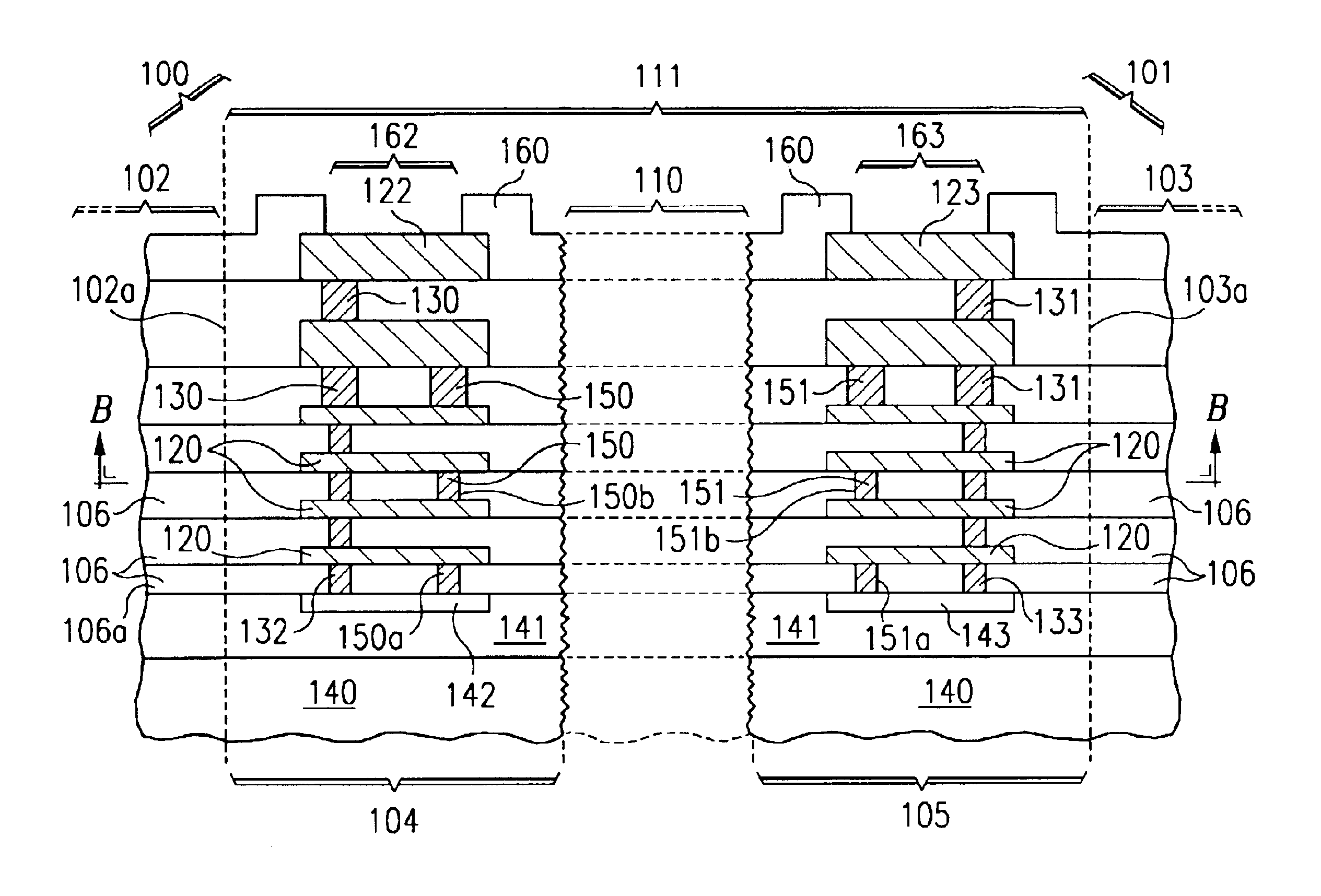
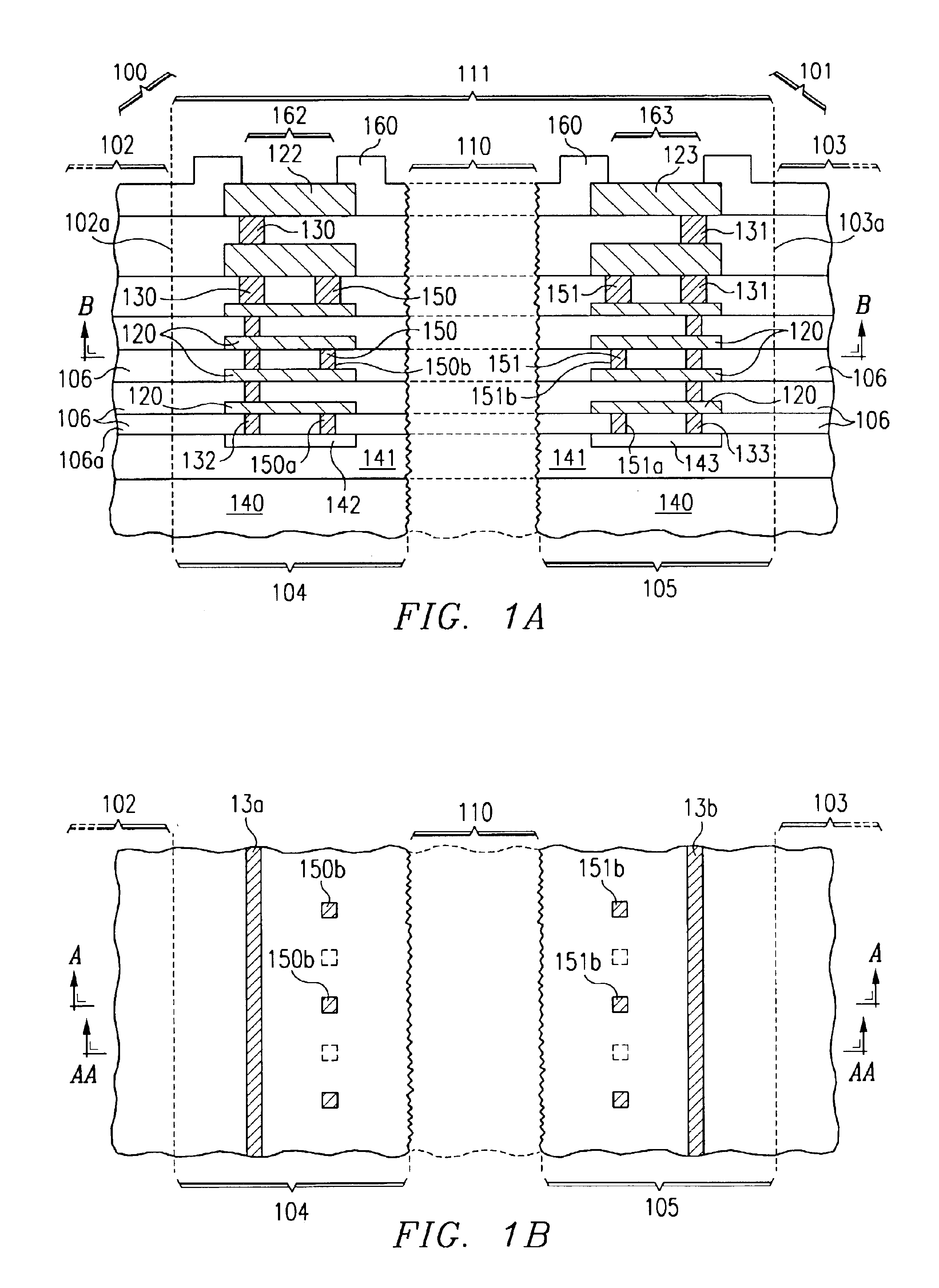
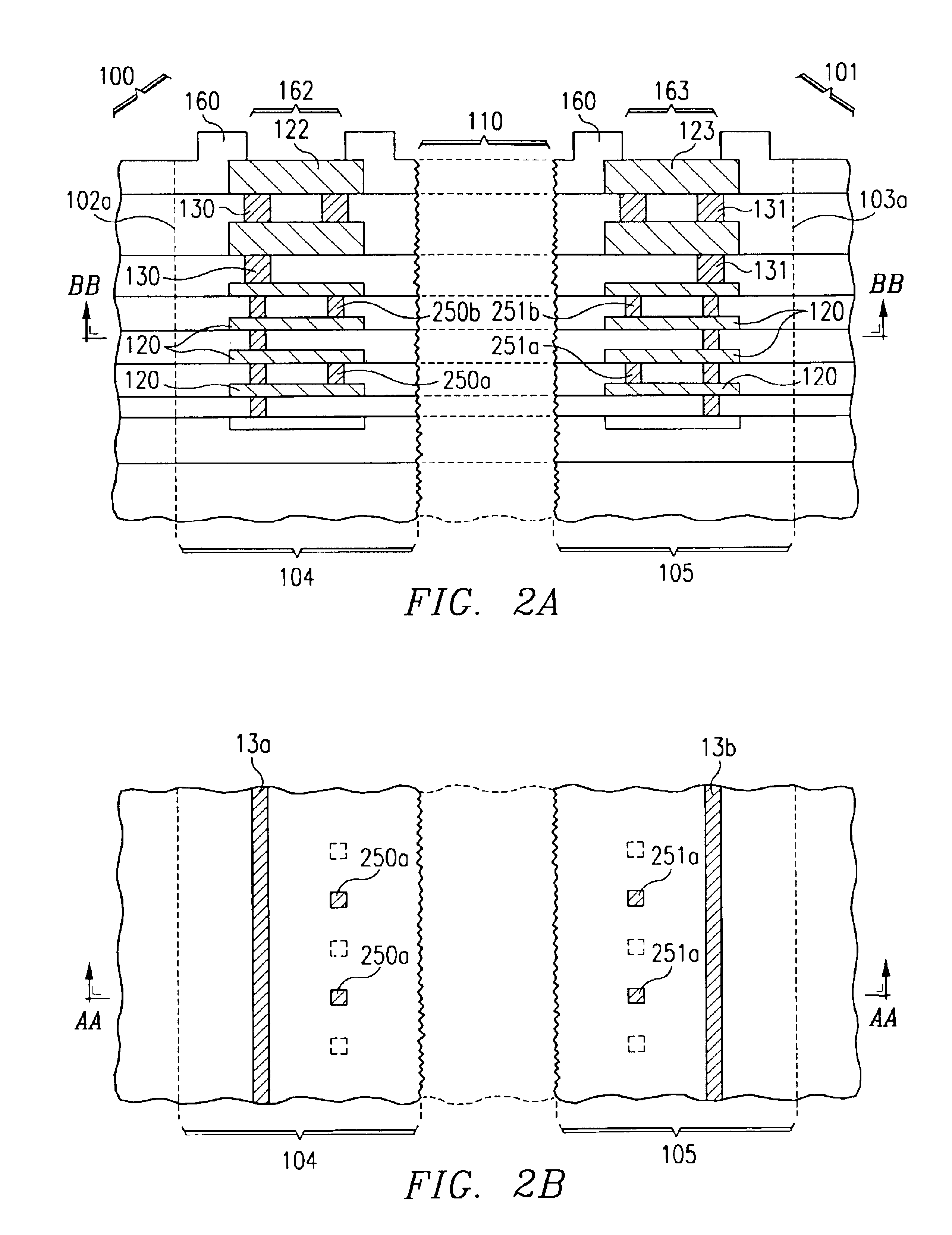
FIG. 1A is a schematic cross section through a small portion of circuit chips 100 and 101 and the dicing line 110 between them. FIG. 1A also shows the cross sections through seal regions 104 and 105, with several embodiments of the invention positioned in each. The first embodiment comprises a seal structure made of a combination of a continuous wall and a discontinuous wall, interconnected by a plurality of patterned, electrically conductive layers 120. These layers are usually made of metal and are formed and patterned simultaneously with the equivalent metal levels of the ICs. As required by the specific IC design, the material of the electrically conductive layer is selected from a group consisting of copper, copper alloy, aluminum, aluminum alloy, tantalum, titanium, tungsten, molybdenum, chromium and compounds thereof.

The part of the seal structure closest to the chip data edge is the continuous barrier wall made by first etching trenches 130 and 131 through the thickness of t...

second embodiment

FIGS. 1A, 2A and 3B also illustrate the present invention, the slot opened in the protective overcoat and reaching from the surface of the overcoat at least to the surface-nearest electrically conductive layer of the sacrificial seal structure. The protective overcoat layer 160 is deposited over the whole wafer in a thickness usually between 0.5 and 1.0 μm. The preferred materialis moisture impermeable silicon nitride, silicon oxy-nitride, or combinations thereof. While the layer is free of pinholes, it is brittle, and cracks originating from dicing line 110 are able to propagate, approximately parallel to the surface, towards the circuit.

Consequently, the invention calls for slots (162 and 163 in FIGS. 1A and 2A, 161 in FIG. 3B) reaching from the surface of overcoat 160 through its whole thickness at least to the surface-nearest electrically conductive layer of the composite structures in the seal regions. In FIGS. 1A and 2A, these conductive layers are designated 122 and 123 in ch...


PUM


Abstract

An integrated circuit wafer, covered by a protective overcoat, comprising an array of integrated circuit chips bordered by seal regions and separated by dicing lines; at least two sets of substantially parallel structures within each of said seal regions, each set extending along the edge of a chip on opposite sides of each said dicing line, respectively; each of said sets comprising at least one continuous barrier wall adjacent each chip, respectively; at least one sacrificial composite structure in combination therewith, between said wall and the center of said dicing line, said composite structure being a discontinuous barrier wall comprising metal rivets interconnecting electrically conductive layers in an alternating manner, whereby said composite structure provides mechanical strength to said sets and simultaneously disperses the energy associated with crack propagation; and at least one slot opened into said protective overcoat, reaching from the surface of said overcoat at least to the surface-nearest electrically conductive layer of said composite structure, whereby cracks propagating in said protective overcoat will be stopped.

Description

FIELD OF THE INVENTIONThe present invention is related in general to the field of semiconductor devices and processes and more specifically to the fabrication of integrated circuit chips protected against potential damage caused by the propagation of cracks initiated by the step of separating semiconductor wafers into individual chips.DESCRIPTION OF THE RELATED ARTWith most semiconductor products, for example integrated circuits, transistors and diodes, a large number of elements are manufactured simultaneously on a large semiconductor wafer of silicon, silicon germanium, gallium arsenide, etc. The semiconductor industry employs the terms “dicing technologies” or “scribing technologies” to refer to those techniques for obtaining a large number of functional chips, or dies, from each semiconductor wafer. Two dicing methods are particularly well known in the art: The grinding-cutting method, using a blade or wire saw, and the scribing method, using a diamond point. Modern silicon tech...

Claims


Application Information

Patent Timeline
IPC IPC(8): H01L23/58H01L23/00H01L21/301H01L23/04
CPCH01L23/562H01L23/585H01L2924/0002H01L2924/00H01L23/04
Inventor WEST, JEFFREY A.GILLESPIE, PAUL M.
Owner TEXAS INSTR INC
Why Eureka
Try Eureka