
Method of making an icosahedral boride structure

a technology of icosahedral boride and structure, applied in the field of icosahedral boride, to achieve the effect of improving film crystallinity and lowering impurity concentrations

Inactive Publication Date: 2005-01-11
UNIVERSITY OF NEW MEXICO +1
View PDF1 Cites 14 Cited by
  • Summary
  • Abstract
  • Description
  • Claims
  • Application Information

AI Technical Summary

Benefits of technology

The present invention provides a method for making thin films of crystalline icosahedral boride on a silicon carbide substrate. This method improves film crystallinity and reduces impurity concentrations. The method involves epitaxially growing layers of boron phosphide or boron arsenide on the silicon carbide substrate using chemical vapor deposition techniques at high temperatures. The resulting thin films can be used for various applications such as semiconductor devices and optical devices.

Problems solved by technology

Crystalline perfection and background impurity issues are linked as crystalline imperfections cause increased contamination incorporation through accelerated diffusion.

Method used


Image

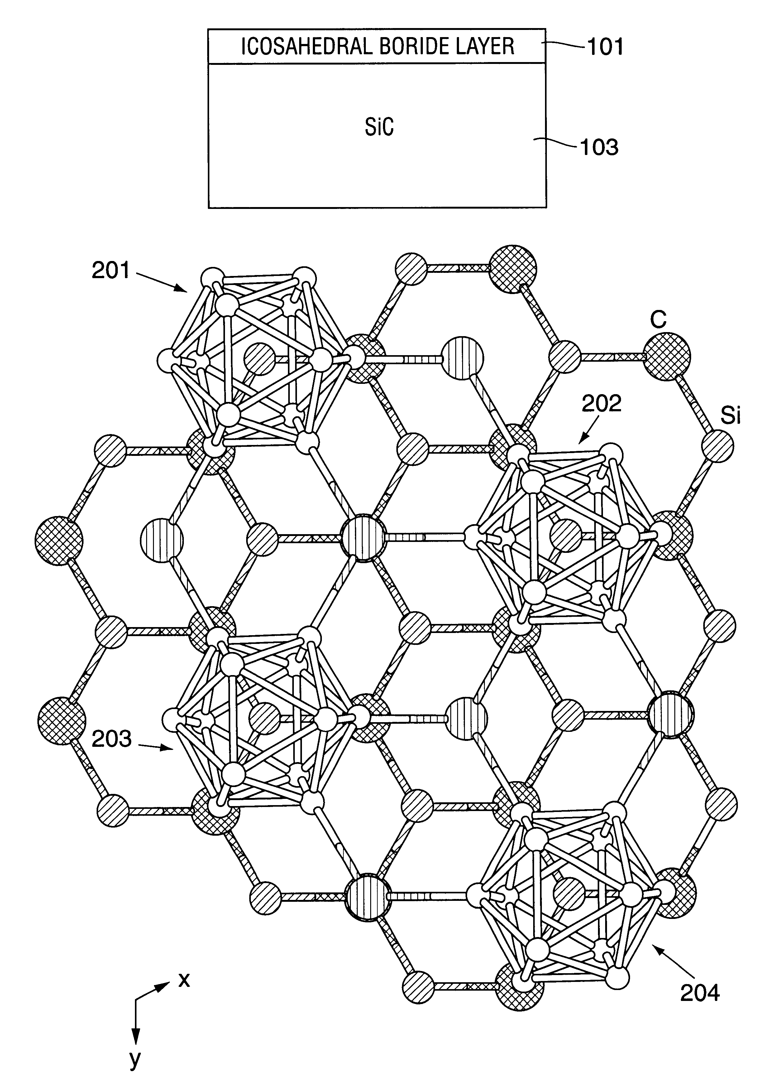
  • Method of making an icosahedral boride structure
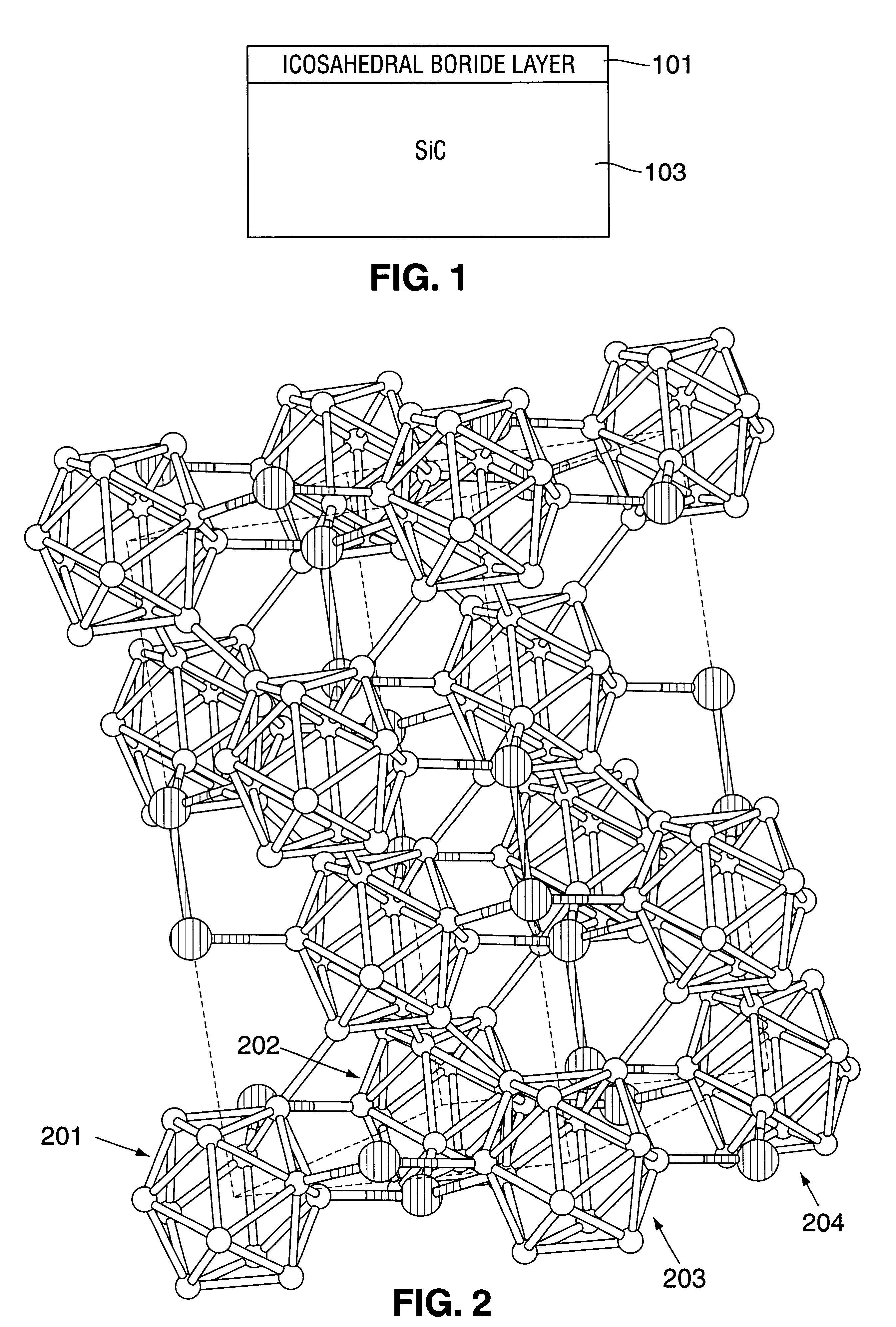
  • Method of making an icosahedral boride structure
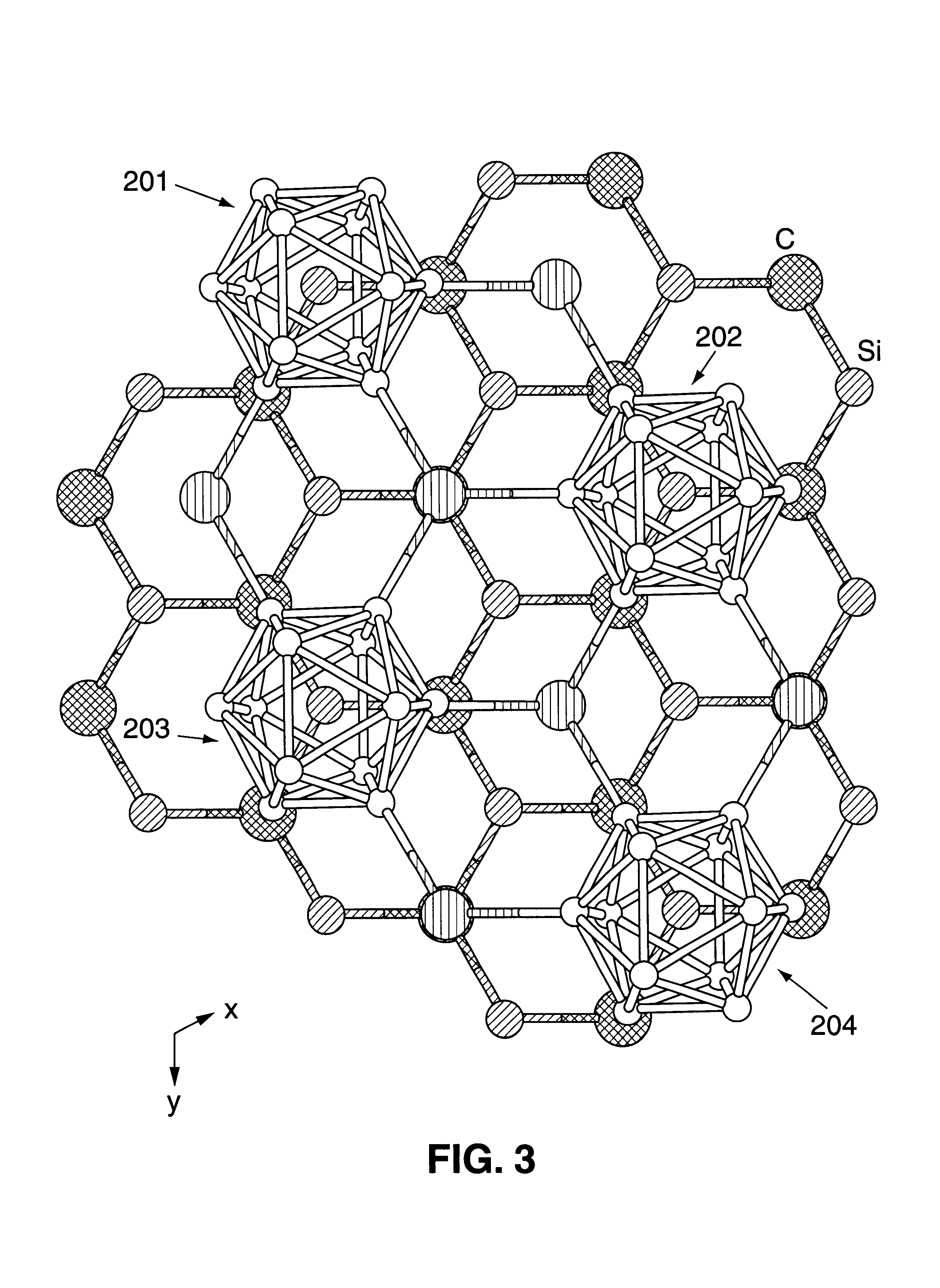
  • Method of making an icosahedral boride structure

Examples


examples

[0030]B12As2 films were deposited on 6H and 3.5° off 6H—SiC substrates in an RF-heated, horizontal-geometry CVD reactor. The SiC substrates were approximately 300 μm thick and were n-type with a bulk resistivity of approximately 0.1 Ω-cm. The substrates were degreased and then dried under nitrogen gas before being loaded into the CVD reactor. CVD films were grown using dilute sources of diborane (1% B2H6 in H2) and arsine (1% AsH3 in H2), which provided boron and arsenic respectively. The flow rates for each of the source gases was 50 sccm with a hydrogen carrier gas flow rate of 5 slm. In order to obtain crystalline films, the deposition temperature should be above 1050° C., preferably in the range of 1100° C. to 1400° C., and more preferably approximately 1150° C. At a deposition temperature of 1150° C. and a pressure of 100 torr, a B12As2 growth rate of 0.2 μm / hr was achieved.

[0031]X-ray diffraction patterns were measured for the films grown on both the on-axis SiC and 3.5 degree...


PUM

PropertyMeasurementUnit
temperatureaaaaaaaaaa

Abstract

A method for fabricating thin films of an icosahedral boride on a silicon carbide (SiC) substrate is provided. Preferably the icosahedral boride layer is comprised of either boron phosphide (B12P2) or boron arsenide (B12As2). The provided method achieves improved film crystallinity and lowered impurity concentrations. In one aspect, an epitaxially grown layer of B12P2 with a base layer or substrate of SiC is provided. In another aspect, an epitaxially grown layer of B12As2 with a base layer or substrate of SiC is provided. In yet another aspect, thin films of B12P2 or B12As2 are formed on SiC using CVD or other vapor deposition means. If CVD techniques are employed, preferably the deposition temperature is above 1050° C., more preferably in the range of 1100° C. to 1400° C., and still more preferably approximately 1150° C.

Description

CROSS-REFERENCES TO RELATED APPLICATIONS[0002]This application is a continuation of U.S. patent application Ser. No. 10 / 277,262, filed Oct. 22, 2002, which is a continuation-in-part of U.S. patent application Ser. No. 09 / 832,278, filed Apr. 9, 2001 now U.S. Pat. No. 6,479,919, which claims the benefit of U.S. Provisional Patent Application Ser. No. 60 / 356,926, filed Oct. 26, 2001, the specifications of which are incorporated herein in their entirety for any and all purposes.GOVERNMENT RIGHTS[0003]This invention was made with Government support under Contract No. DE-AC04-94AL85000 awarded by the United States Department of Energy. The Government has certain rights in the invention.BACKGROUND OF THE INVENTION[0004]The icosahedral borides, such as boron phosphide (B12P2) and boron arsenide (B12As2), are hard and chemically inert solids that exhibit exceptional radiation tolerance due, at least in part, to the strong bonding within the boron icosahedra. It has been suggested that if the...

Claims


Application Information

Patent Timeline
Patent Type & Authority Patents(United States)
IPC IPC(8): G21H1/06G21H1/00G21H1/02
CPCG21H1/02G21H1/06G21Y2002/201Y10S438/931G21Y2004/10G21Y2004/30G21Y2002/304
Inventor HERSEE, STEPHEN D.WANG, RONGHUAZUBIA, DAVIDASELAGE, TERRANCE L.EMIN, DAVID
Owner UNIVERSITY OF NEW MEXICO
Learn More