Group III nitride compound semiconductor device and method for producing the same

a technology of compound semiconductors and nitride, which is applied in the direction of semiconductor devices, basic electric elements, electrical equipment, etc., can solve the problems of long production time, crystallinity degradation of semiconductors, and bowing problems, so as to reduce the labor required for adjusting the temperature and reduce the production time

Inactive Publication Date: 2005-01-11
TOYODA GOSEI CO LTD
View PDF12 Cites 124 Cited by
  • Summary
  • Abstract
  • Description
  • Claims
  • Application Information

AI Technical Summary

Benefits of technology

[0030]In the producing method configured as described above, a low-temperature sedimentary layer is not formed in the same manner as that in the background art, but an undercoat layer having a surface of a texture structure is formed and then a group III nitride compound semiconductor layer is grown on the undercoat layer. Hence, the growth of the group III nitride compound semiconductor layer as the next step can be performed without reduction of the substrate temperature required in the

Problems solved by technology

It is therefore, a matter of course that a long time is required for production.
In addition, it is undesirable from the point of view of thermal efficiency.
However, a bowing problem hereinafter described occurs if the group III nitride compound semiconductor layer (for example, an AlN layer the same as the low-temperature sedimentary layer) is directly grown on the substrate at a high temperatu

Method used


Image

  • Group III nitride compound semiconductor device and method for producing the same
  • Group III nitride compound semiconductor device and method for producing the same
  • Group III nitride compound semiconductor device and method for producing the same

Examples


first embodiment

[0088]FIG. 5 shows the structure of the light-emitting diode 10 according to a

LayerComposition: DopantLight-transmissiblep-GaN: Mgelectrode layer 17p-type layer 16Layer 15 includingincluding InGaN layera light emitting layern-GaN: Sin-type layer 14Growth suppressingSiO2material layer 13Undercoat layer 12AlNSubstrate 11sapphire (surface a)

[0089]The n-type layer 14 may be of a double-layered structure with an n− layer of low electron density on the layer 15 side and an n+ layer of high electron density on the undercoat layer 12 side. The latter is called n-type contact layer.

[0090]The layer 15 is not limited to the multiple quantum well structure. A single hetero type structure, a double hetero type structure, a homo-junction type structure, or the like, may be used as the configuration of the light-emitting device.

[0091]A group III nitride compound semiconductor layer doped with an acceptor such as magnesium and having a wide band gap may be interposed between the layer 15 and the p-...

second embodiment

[0110]Next, the present invention will be described below.

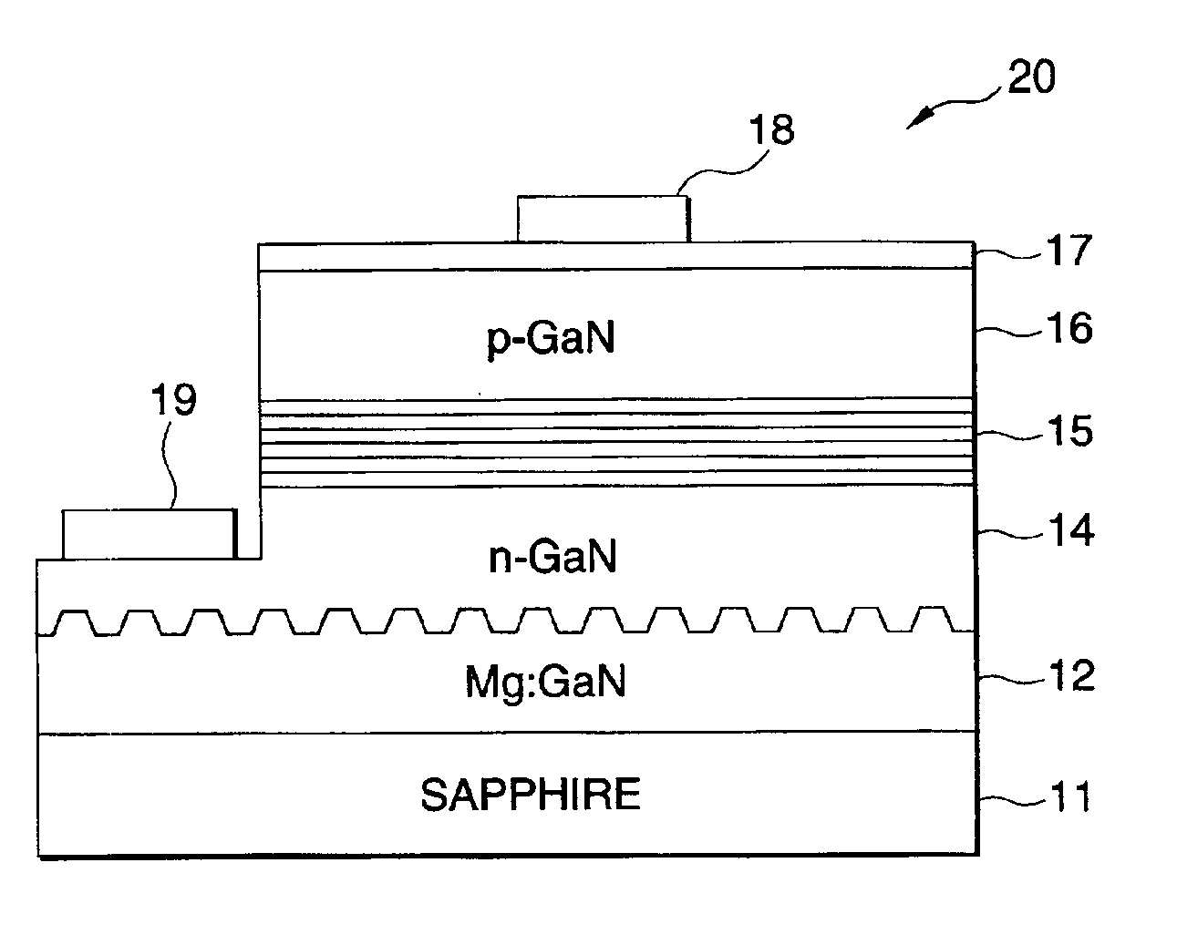
[0111]The embodiment shows a light-emitting diode 20. FIG. 7 shows the configuration of the light-emitting diode 20. In FIG. 7, parts the same as those in FIG. 5 are referenced correspondingly for the purpose of omission of duplicated description.

[0112]The specification of each layer is as follows.

LayerComposition: DopantLight-transmissiblep-GaN: Mgelectrode layer 17p-type layer 16Layer 15 includingn-GaN: Sia light emitting layern-type layer 14Undercoat layer 12GaN: MgSubstrate 11sapphire (surface a)

[0113]The light-emitting diode configured as described above is produced as follows.

[0114]First, while a hydrogen gas is circulated in a reactor of an MOCVD apparatus, the sapphire substrate is heated to 1130° C. to thereby clean the surface of the sapphire substrate.

[0115]Then, while TMG, NH3 and CP2Mg are introduced at the substrate temperature, an undercoat layer 12 of GaN doped with Mg is grown by an MOCVD method. On this occa...

third embodiment

[0121]FIG. 9 shows a light-emitting diode 30 according to the present invention. In FIG. 9, parts the same as those in FIGS. 5 and 7 are referenced correspondingly for the purpose of omission of duplicated description.

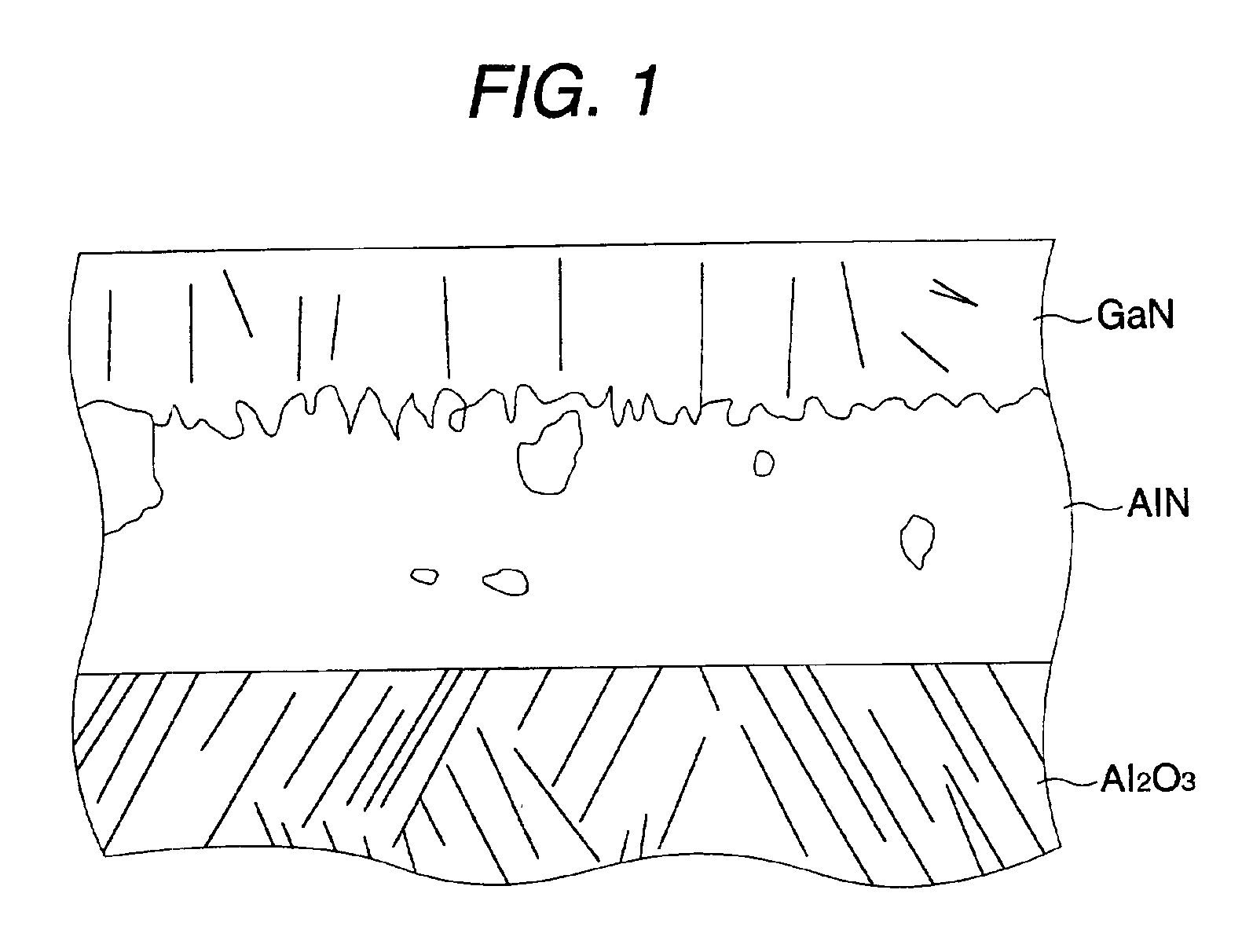
[0122]In the light-emitting diode 30 according to this embodiment, a sedimentary layer 31 of AlN is interposed between the sapphire substrate 11 and the undercoat layer 35.

[0123]The specification of each layer is as follows.

LayerComposition: DopantLight-transmissiblep-GaN: Mgelectrode layer 17p-type layer 16Layer 15 includingn-GaN: Sia light emitting layern-type layer 14Undercoat layer 35GaN: MgSedimentary layer 31AlNSubstrate 11sapphire (surface a)

[0124]The light-emitting diode 30 configured as described above is produced as follows.

[0125]First, reactive sputtering using an aluminum target in a nitrogen gas import atmosphere is made at a sapphire substrate temperature in a range of from 300 to 500° C. by an argon gas sputtering apparatus. The sapphire substrate having...


PUM


Abstract

An AlN layer having a surface of a texture structure is formed on a sapphire substrate. Then, a growth suppressing material layer is formed on the AlN layer so that the AlN layer is partially exposed to the outside. Then, group III nitride compound semiconductor layers are grown on the AlN layer and on the growth suppressing material layer by execution of an epitaxial lateral overgrowth method. Thus, a group III nitride compound semiconductor device is produced. An undercoat layer having convex portions each shaped like a truncated hexagonal pyramid is formed on a substrate. Group III nitride compound semiconductor layers having a device function are laminated successively on the undercoat layer.

Description

BACKGROUND OF THE INVENTION[0002]1. Field of the Invention[0003]The present invention relates to a group III nitride compound semiconductor device and a method for producing thereof. Particularly, it relates to improvement of a producing method using an epitaxial lateral overgrowth method as a method for growing a group III nitride compound semiconductor film.[0004]The present application is based on Japanese Patent Applications Nos. 2000-189391 and 2000-191780, which are incorporated herein by reference.[0005]2. Description of the Related Art[0006]A so-called epitaxial lateral overgrowth method is known as a method for growing a group III nitride compound semiconductor layer. For example, in the epitaxial lateral overgrowth method as introduced in Unexamined Japanese Patent Publication No. Hei. 10-312971, a mask layer of a growth suppressing material such as SiO2 is patterned on an undercoat by a photolithography method and a wet etching method in advance, so that a group III nitri...

Claims


Application Information

Patent Timeline
IPC IPC(8): H01L21/02H01L21/20H01L33/00H01L33/32
CPCH01L21/0237H01L21/0242H01L21/02458H01L21/02494H01L33/32H01L21/02642H01L21/02647H01L33/007H01L21/0254
Inventor SHIBATA, NAOKICHIYO, TOSHIAKISENDA, MASANOBUITO, JUNWATANABE, HIROSHIASAMI, SHINYAASAMI, SHIZUYO
Owner TOYODA GOSEI CO LTD
Why Eureka
Try Eureka