Semiconductor device
- Summary
- Abstract
- Description
- Claims
- Application Information
AI Technical Summary
Benefits of technology
Problems solved by technology
Method used
Image

Examples
first embodiment
(First Embodiment)
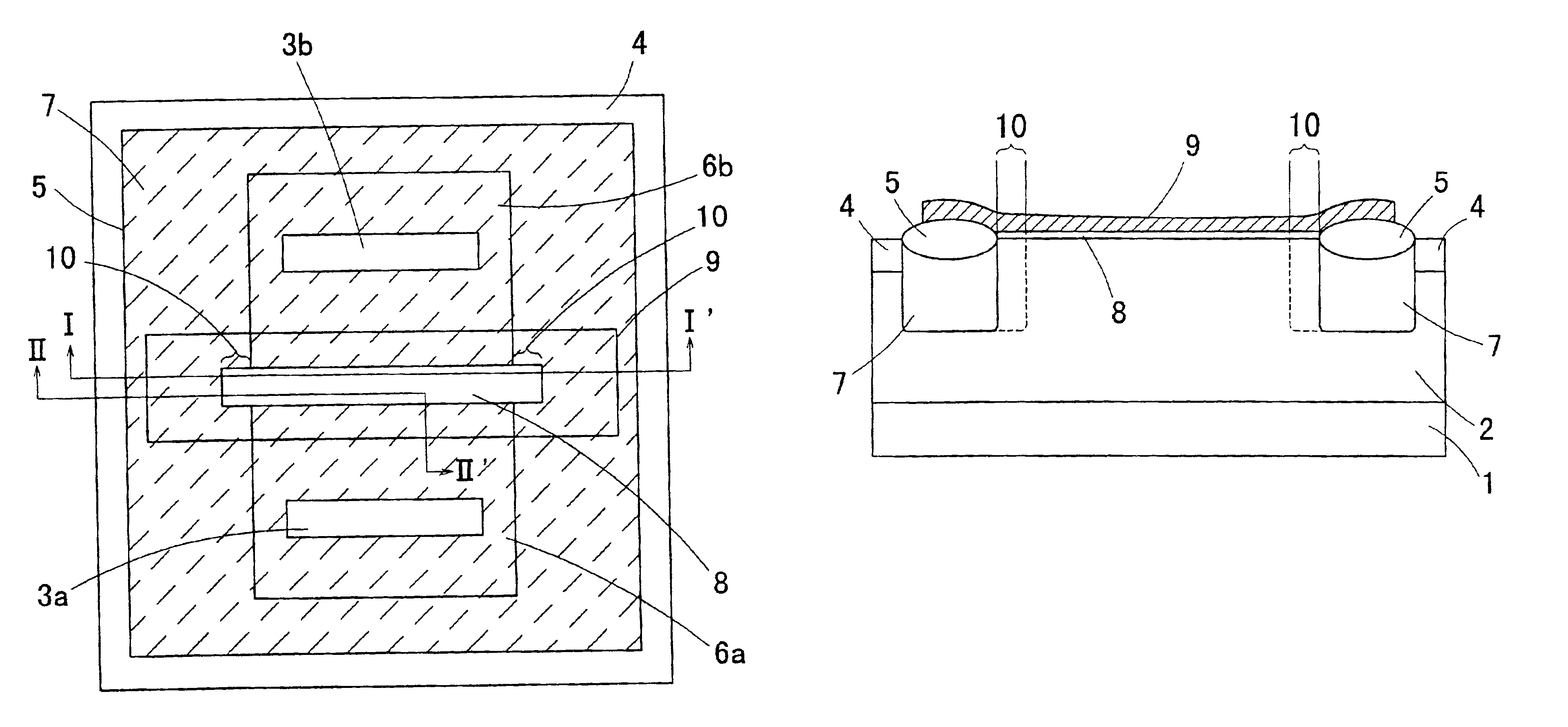
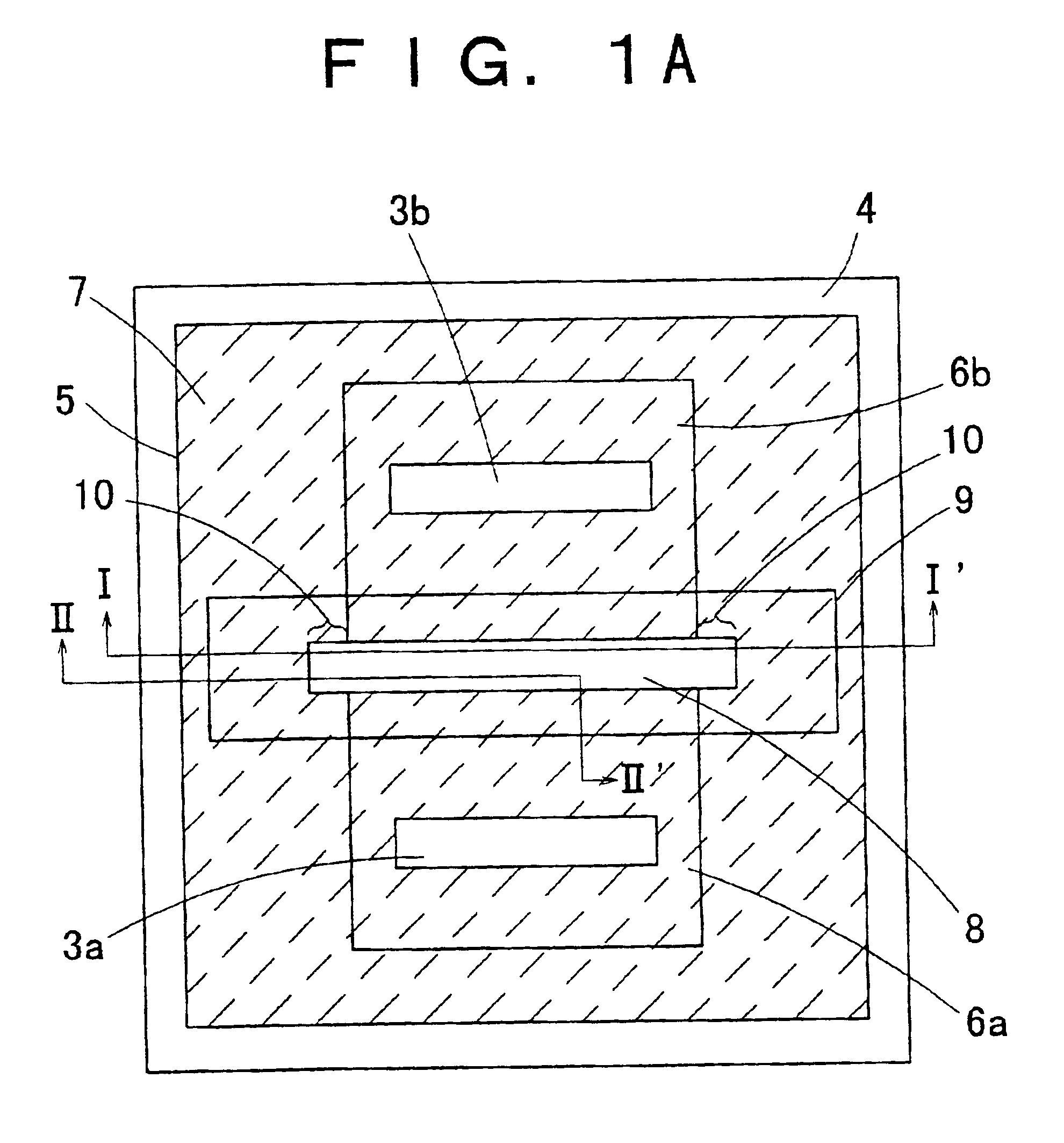
The structure of an N-channel high voltage transistor which is a semiconductor device according to a first embodiment of the present invention is shown in FIGS. 1A to 1C. FIG. 1A is a perspective plan view of the high voltage transistor according to the first embodiment. FIG. 1B is a cross-sectional view taken on the line I-I′ of FIG. 1A. FIG. 1C is a cross-sectional view taken on the line II-II′ of FIG. 1A. The chain double-dashed line S in FIG. 1C represents the bent part of the line II-II′ of FIG. 1A.
A P-type well 2 is present on the surface of a P-type substrate 1. N-type source and drain diffusion layers 3a and 3b, a P-type guard band diffusion layer 4 and a LOCOS oxide film are present on the surface of the P-type well 2. N-type offset source and drain diffusion layers 6a and 6b and a P-type diffusion layer 7 are present below the LOCOS oxide film 5. The P-type diffusion layer 7 is necessary for acting as a channel stopper region below the LOCOS oxide film 5....
second embodiment
(Second Embodiment)
The structure of an N-channel high voltage transistor which is a semiconductor device according to a second embodiment of the present invention is shown in FIGS. 2A to 2C. FIG. 2A is a perspective plan view of the high voltage transistor according to the second embodiment. FIG. 2B is a cross-sectional view taken on the line I-I′ of FIG. 2A. FIG. 2C is a cross-sectional view taken on the line II-II′ of FIG. 2A. The chain double-dashed line S in FIG. 2C represents the bent part of the line II-II′ of FIG. 2A.
In the second embodiment, like in the first embodiment, a P-type well 2 is present on the surface of a P-type substrate 1. N-type source and drain diffusion layers 3a and 3b, a P-type guard band diffusion layer 4 and a LOCOS oxide film 5 are present on the surface of the P-type well 2. N-type offset source and drain diffusion layers 6a and 6b and a P-type diffusion layer 7 are present below the LOCOS oxide film 5. A polysilicon gate electrode 9 is present so as t...
PUM
 Abstract
Description
Claims
Application Information
 - R&D
- Intellectual Property
- Life Sciences
- Materials
- Tech Scout
- Unparalleled Data Quality
- Higher Quality Content
- 60% Fewer Hallucinations
Browse by: Latest US Patents, China's latest patents, Technical Efficacy Thesaurus, Application Domain, Technology Topic, Popular Technical Reports.
© 2025 PatSnap. All rights reserved.Legal|Privacy policy|Modern Slavery Act Transparency Statement|Sitemap|About US| Contact US: help@patsnap.com