Variable gain amplifier

a variable gain amplifier and amplifier technology, applied in amplifier combinations, automatic tone/bandwidth control, gain control, etc., can solve the problems of high power requirement, inability to easily integrate, and inability to fully integrate single chip receivers, etc., to achieve good impedance matching, good noise performance, and the effect of reducing the gain of the variable gain amplifier

Inactive Publication Date: 2005-01-11
ANALOG DEVICES INC
View PDF7 Cites 18 Cited by
  • Summary
  • Abstract
  • Description
  • Claims
  • Application Information

AI Technical Summary

Benefits of technology

The advantages of the invention are many. In particular, the provision of the shunt-shunt feedback circuit and the passive shunt impedance circuit provide particularly good impedance matching for matching the impedance of the variable gain amplifier with the source impedance. By providing the shunt-shunt feedback circuit and the passive shunt impedance circuit, the input impedance of the variable gain amplifier can be maintained within a relatively narrow predetermined input impedance range as the gain of the variable gain amplifier is varied. In particular, the shunt-shunt feedback circuit can provide sufficient shunt impedance at the main input terminal for maintaining the input impedance of the variable gain amplifier within the predetermined input impedance range while the gain of the variable gain amplifier is being varied at the high gain end of the gain range. As the gain of the variable gain amplifier is then further reduced, shunt impedance can be shunted to the main input terminal from the passive shunt impedance circuit for maintaining the input impedance of the variable gain amplifier within the predetermined input impedance range for the lower end of the gain range of the amplifier.
The feedback amplifier of the shunt-shunt feedback circuit provides relatively good noise performance, which is significantly better than the noise performance which can be achieved from the passive shunt impedance circuit. However, distortion of the signal is stronger when the feedback amplifier of the shunt-shunt feedback circuit is active. The passive shunt impedance circuit causes significantly less distortion than the feedback amplifier, due to the fact that the shunt impedance elements of the passive shunt impedance circuit are passive elements, namely, resistive elements. However, since the shunt-shunt feedback circuit is activated when the variable gain amplifier is operating at the high end of the gain range only, the level of the input signal would generally be relatively low, and thus distortion of the signal is not particularly critical, and is not as critical as when the level of the input signal is higher, for example, when the variable gain amplifier is operating at the lower end of the gain range. Additionally, the fact that the feedback amplifier provides good noise performance is also particularly important when the signal is a relatively low level signal. However, when the variable gain amplifier is operating at the low end of the gain range, the input signal, in general, is at a relatively higher level where minimum distortion is required, and noise performance is not as important. Thus, since at the low end of the gain range of the variable gain amplifier, the shunt-shunt feedback circuit will be deactivated, and the additional shunt impedance will be obtained from the passive shunt impedance circuit, which causes little distortion, and additionally, once the gain of the variable gain amplifier is operating in the low end of the gain range, its input referred noise is more and more dominated by the actual signal attenuation than by the intrinsic noise of the amplifier itself. Thus, any additional thermal noise at the input of the variable gain amplifier resulting from the passive shunt impedance circuit becomes insignificant. Acc...

Problems solved by technology

However, so far such a fully integrated single chip receiver has not yet been successfully provided.
One of the difficulties in providing such a single chip integrated receiver lies in the requirement of providing a suitable variable gain amplifier, and in particular, a variable gain amplifier with low noise characteristics in CMOS which is suitable for terrestrial digital television signals.
While such circuits provide good performance characteristics, they are not readily integratable, and have a high power requirement.
However, the variation range of the source degeneration resistance, and hence linearity improvement is limited by headroom constraints, particularly in a low voltage environment.
In order to meet peak two-one third order intercept point (IIP3) requirements, a high initial linearity is required, which results in a high power consumption.
However, such performance is insufficient for cable and terrestrial digital television applications.
However, a ...

Method used


Image

  • Variable gain amplifier
  • Variable gain amplifier
  • Variable gain amplifier

Examples


Embodiment Construction

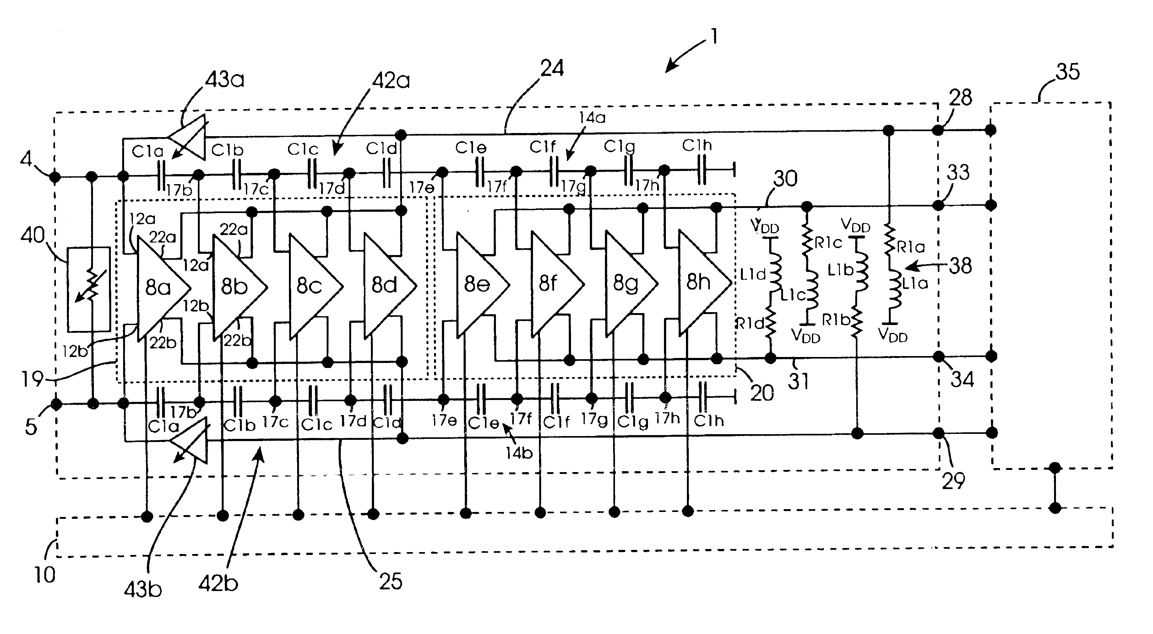
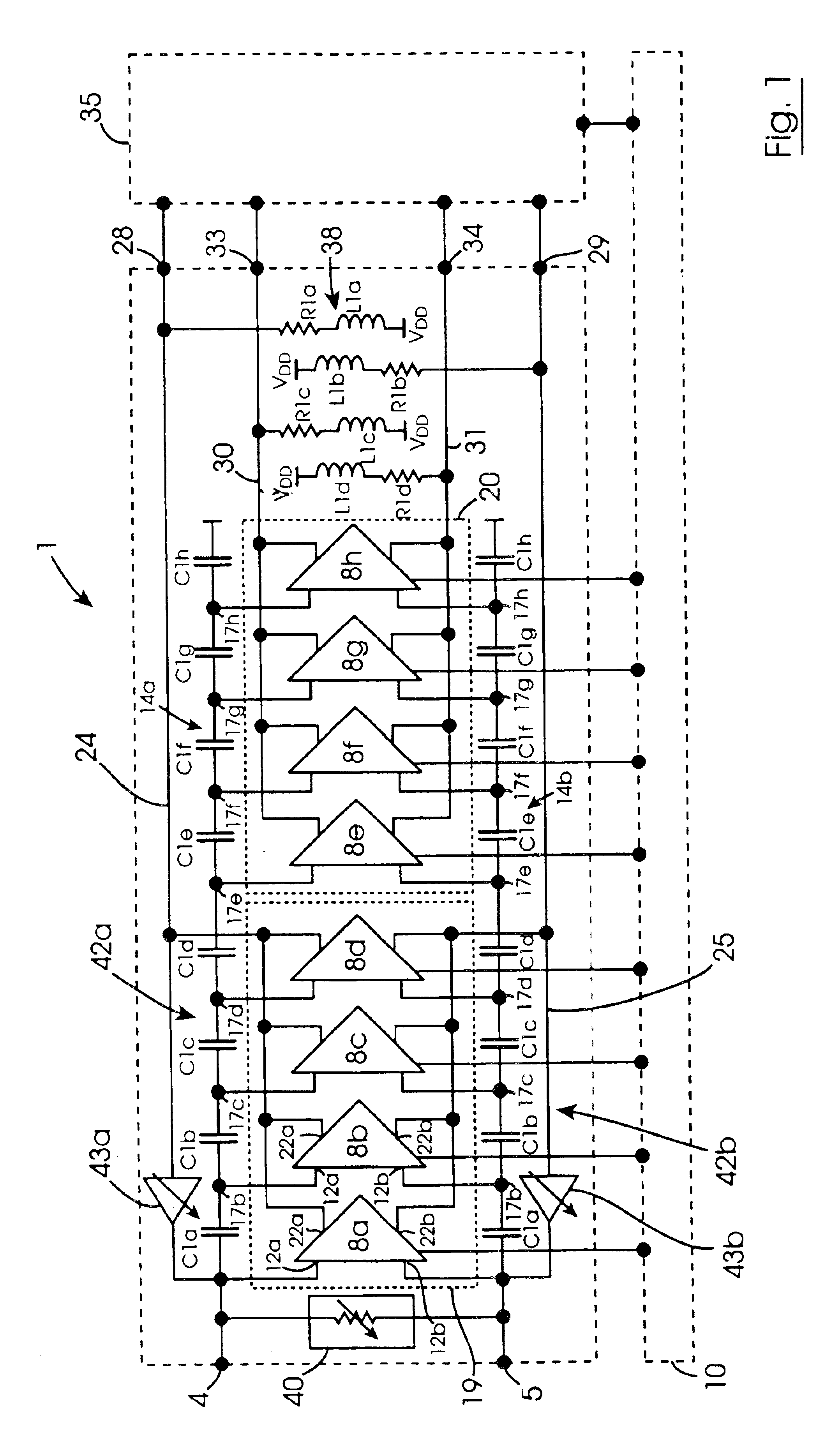
Referring to the drawings and initially to FIG. 1, there is illustrated a broadband radio frequency differential variable gain multi-stage amplifier according to the invention, indicated generally by the reference numeral 1. The variable gain amplifier 1 is an amplifier with low noise characteristics, and is particularly suitable for amplifying digital television signals from an antenna and / or a communal cable system. Prior to being applied to the variable gain amplifier 1, the signals from the antenna and / or cable system are filtered by a band selection filter (not shown) and are converted into a differential form in order to maintain symmetry to ground.

The variable gain amplifier 1 comprises a pair of differential input terminals, namely, a positive main input terminal 4, and a negative main input terminal 5 for receiving the respective positive and negative ends of the differential signal from the band selection filter (not shown). N identical gain stages, in this embodiment of t...


PUM


Abstract

A differential variable gain amplifier (1) comprises eight identical variable gain stages (8a to 8d) which are arranged in two groups, namely, a high gain group (19) and a low gain group (20). The first gain stage (8a) is coupled directly to a pair of positive and negative main input terminals (4,5) for receiving a differential input signal to be amplified. A pair of voltage divider impedance chains (14) comprising identical capacitors (C1a to C1g) define taps (17b to 17h) through which the input signal is applied to the corresponding gain stages (8b to 8h) in progressive steps of attenuation. Each gain stage (8) comprises a pair of identical variable gain amplifier elements (11) which amplify the respective positive and negative ends of the differential input signal. Only one of the gain stages (8a to 8h) is selected at any one time by a control circuit 10. The outputs from the gain stages (8) of the high gain group (19) are applied to positive and negative high gain output terminals (28,29). The output of the gain stages (8) of the low gain group (20) are applied on positive and negative low gain output terminals (33,34). A pair of selectively activatable shunt-shunt feedback circuits (42a,42b) each comprising a variable gain feedback amplifier (43a,43b) provide variable shunt impedance at the main input terminals (4,5) for maintaining the input impedance of the variable gain amplifier (1) within a predetermined input impedance range as the gain of the variable gain amplifier (1) is varied, and when the variable gain amplifier (1) is operating at the high end of its gain range. A passive shunt impedance circuit (40) comprising a plurality of resistive shunt impedance elements are independently selectively shuntable across the main input terminals (4,5) for maintaining the input impedance of the variable gain amplifier (1) within the predetermined input impedance range when the variable gain amplifier (1) is operating at the low gain end of its gain range.

Description

FIELD OF THE INVENTIONThe present invention relates to a variable gain amplifier, and in particular to a broadband radio frequency variable gain amplifier, which is suitable for use in the processing of, for example, cable and terrestrial digital television signals.BACKGROUND TO THE INVENTIONWith the expansion of digital television, signal processing equipment which can process digital television signals transmitted over cable and over terrestrial channels is required. The provision of a single chip receiver capable of processing both types of digital television signals is desirable. Furthermore, the implementation of such a single chip receiver in CMOS technology is desirable due to the repeatability and cost advantage which can be achieved using CMOS processes. However, so far such a fully integrated single chip receiver has not yet been successfully provided. One of the difficulties in providing such a single chip integrated receiver lies in the requirement of providing a suitabl...

Claims


Application Information

Patent Timeline
IPC IPC(8): H03G1/00
CPCH03F3/45475H03G1/0088H03G1/0023H03F2203/45134
Inventor RETZ, GUIDOBURTON, DAVID PHILIP
Owner ANALOG DEVICES INC
Why Eureka
Try Eureka