Low defect density silicon having a vacancy-dominated core substantially free of oxidation induced stacking faults

a low defect density, vacancy-dominated core technology, applied in the field of semiconductor grade single crystal silicon preparation, can solve the problems of increasing the number of defects in single crystal silicon form, the formation of agglomeration intrinsic point defects, so as to achieve the effect of reducing concentration

Inactive Publication Date: 2005-01-25
GLOBALWAFERS CO LTD
View PDF80 Cites 29 Cited by
  • Summary
  • Abstract
  • Description
  • Claims
  • Application Information

AI Technical Summary

Benefits of technology

Among the features of the present invention, therefore, is the provision of single crystal silicon, in ingot or wafer form, having an axially symmetric region extending radially inward from the lateral surface of the ingot or circumferential edge of the wafer, of a substantial radial width, wherein silicon self-interstitials are the predominant intrinsic point defect and which is substantially free of agglomerated intrinsic point defects; the provision of such a single crystal silicon ingot or wafer having another axially symmetric region, extending radia...

Problems solved by technology

It is now recognized that a number of defects in single crystal silicon form in the growth chamber as the ingot cools from the temperature of solidification.
Upon cooling to below this threshold temperature, a reaction or agglomeration event occurs, resulting in the formation of agglomerated intrinsic point defects.
Such defects are not responsible for gate oxide integrity failures, an important wafer performance criterion, but they are widely recognized to be the cause of other types of device failures usually associated with current leakage problems.
While these values are relatively low, agglomerated intrinsic point defects are of rapidly increasing importance to device manufacturers and, in fact, are now seen as yield-limiting factors in device fabrication processes.
While the ingot ...

Method used


Image

  • Low defect density silicon having a vacancy-dominated core substantially free of oxidation induced stacking faults
  • Low defect density silicon having a vacancy-dominated core substantially free of oxidation induced stacking faults
  • Low defect density silicon having a vacancy-dominated core substantially free of oxidation induced stacking faults

Examples


example

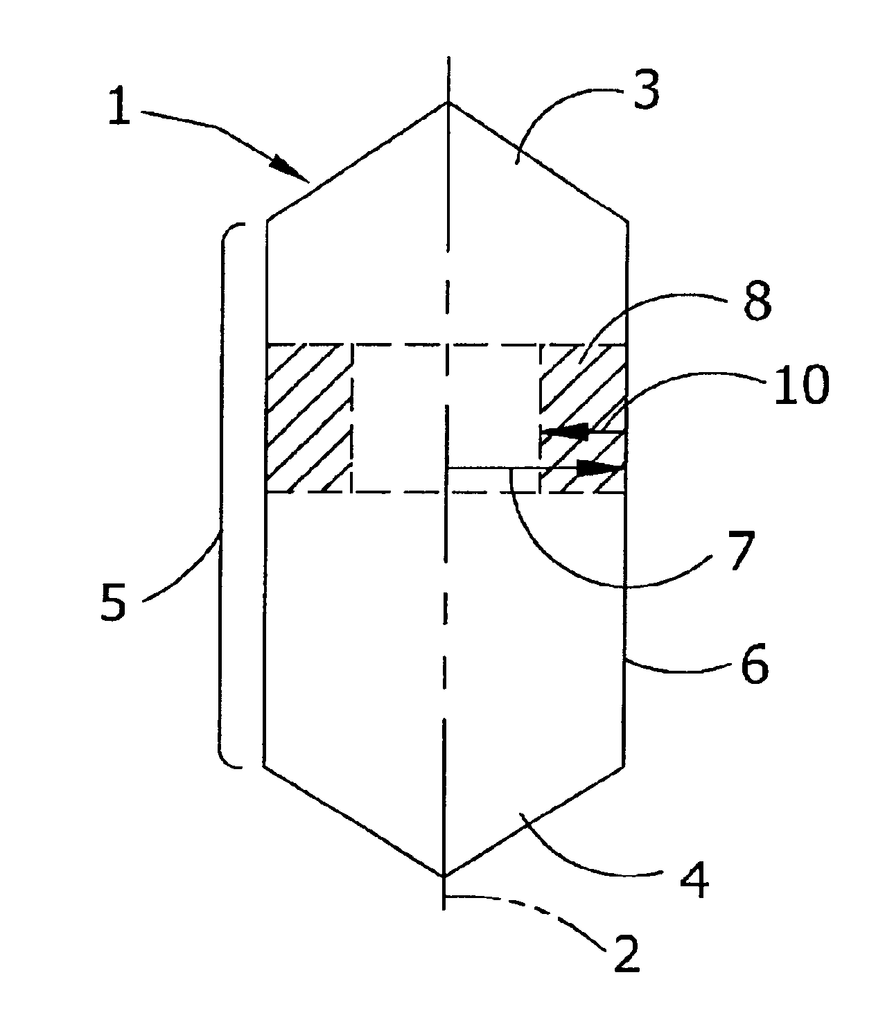
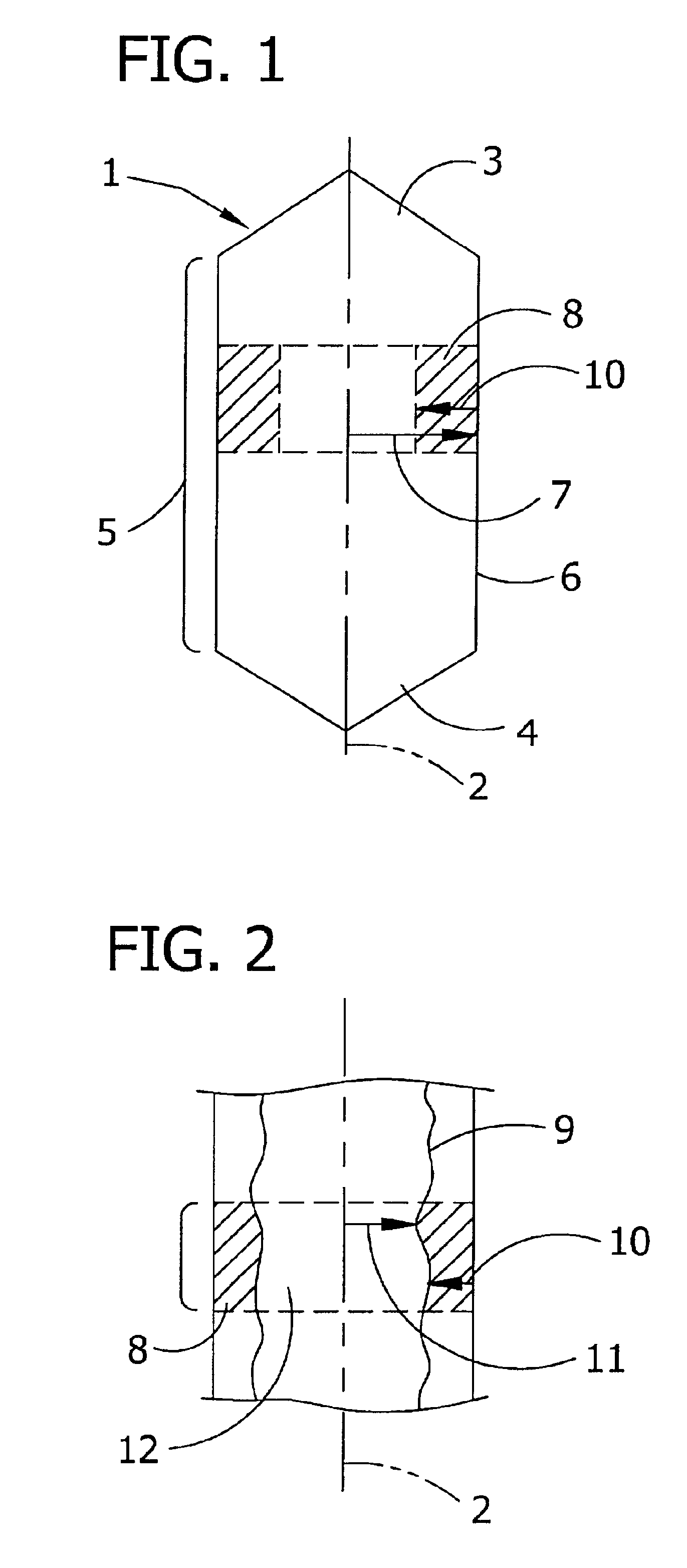
In accordance with the present invention, a series of single crystal silicon ingots having a diameter of about 200 mm were grown in accordance with the Czochralski method, a portion of the series being grown in a crystal puller which did not possess an additional apparatus for cooling the solidified ingot and a portion being grown in a crystal pulling apparatus which did (e.g., a crystal puller having a cooling jacket positioned in the transition area of the puller, such as the one described herein). Each ingot was generally grown using the same growth conditions, such that each had a segment comprising an interstitial-dominated, axially symmetric region which was substantially free of agglomerated defects and which was concentric about a vacancy-dominated, axially symmetric region (the width of each axially symmetric region, from one ingot to the next, being approximately the same). The only significant difference between the ingots, or the ingot segments, that were grown and analy...


PUM


Abstract

The present invention relates to a process for preparing a single crystal silicon ingot, as well as to the ingot or wafer resulting therefrom. The process comprises controlling (i) a growth velocity, v, (ii) an average axial temperature gradient, G0, and (iii) a cooling rate of the crystal from solidification to about 750° C., in order to cause the formation of a segment having a first axially symmetric region extending radially inward from the lateral surface of the ingot wherein silicon self-interstitials are the predominant intrinsic point defect, and a second axially symmetric region extending radially inward from the first and toward the central axis of the ingot. The process is characterized in that v, G0 and the cooling rate are controlled to prevent the formation of agglomerated intrinsic point defects in the first region, while the cooling rate is further controlled to limit the formation of oxidation induced stacking faults in a wafer derived from this segment, upon subjecting the wafer to an oxidation treatment otherwise suitable for the formation of such faults.

Description

BACKGROUND OF THE INVENTIONThe present invention generally relates to the preparation of semiconductor grade single crystal silicon which is used in the manufacture of electronic components. More particularly, the present invention relates to single crystal silicon ingots and wafers, as well as a process for the preparation thereof, having (i) an outer, axially symmetric region wherein silicon interstitials are the predominant intrinsic point defect and which is devoid of agglomerated intrinsic point defects, surrounding (ii) an inner, axially symmetric region wherein silicon lattice vacancies are the predominant intrinsic point defect and which is substantially free of nuclei which lead to the formation of oxidation induced stacking faults.Single crystal silicon, which is the starting material in most processes for the fabrication of semiconductor electronic components, is commonly prepared by the so-called Czochralski (“Cz”) method. In this method, polycrystalline silicon (“polysi...

Claims


Application Information

Patent Timeline
IPC IPC(8): C30B15/00C30B29/06C30B15/20C30B33/02
CPCC30B15/20C30B15/203C30B29/06C30B15/206Y10T428/21C30B15/00
Inventor KIM, CHANG BUMKIMBEL, STEVEN L.LIBBERT, JEFFREY L.BANAN, MOHSEN
Owner GLOBALWAFERS CO LTD
Why Eureka
Try Eureka