


Quick Research
Generate reliable direction feasibility study reports for your R&D in just a few steps.

Technical Q&A
Discover and master advanced knowledge NOW. Basics, ideas, possibilities, all at once.

Find Solutions
As an expert in R&D theories, this can generate solutions to your technical problems instantly.

Evaluate Feasibility
Analyze your overall solution with one click, know your potential R&D risks in advance.

Monitor Landscape
Get weekly tech updates, stay abreast of the latest tech innovations and key insights.
Glass substrate assembly, semiconductor device and method of heat-treating glass substrate
a technology of glass substrate and semiconductor device, which is applied in the field of glass substrate, can solve the problems of substrate shrinkage caused by thermal treatment, the upper limit of the thermal treatment temperature is restricted, and the manufacturing process is a great obstacle to the manufacturing process
- Summary
- Abstract
- Description
- Claims
- Application Information
AI Technical Summary
Benefits of technology
Problems solved by technology
Method used
Image

Examples
example 2
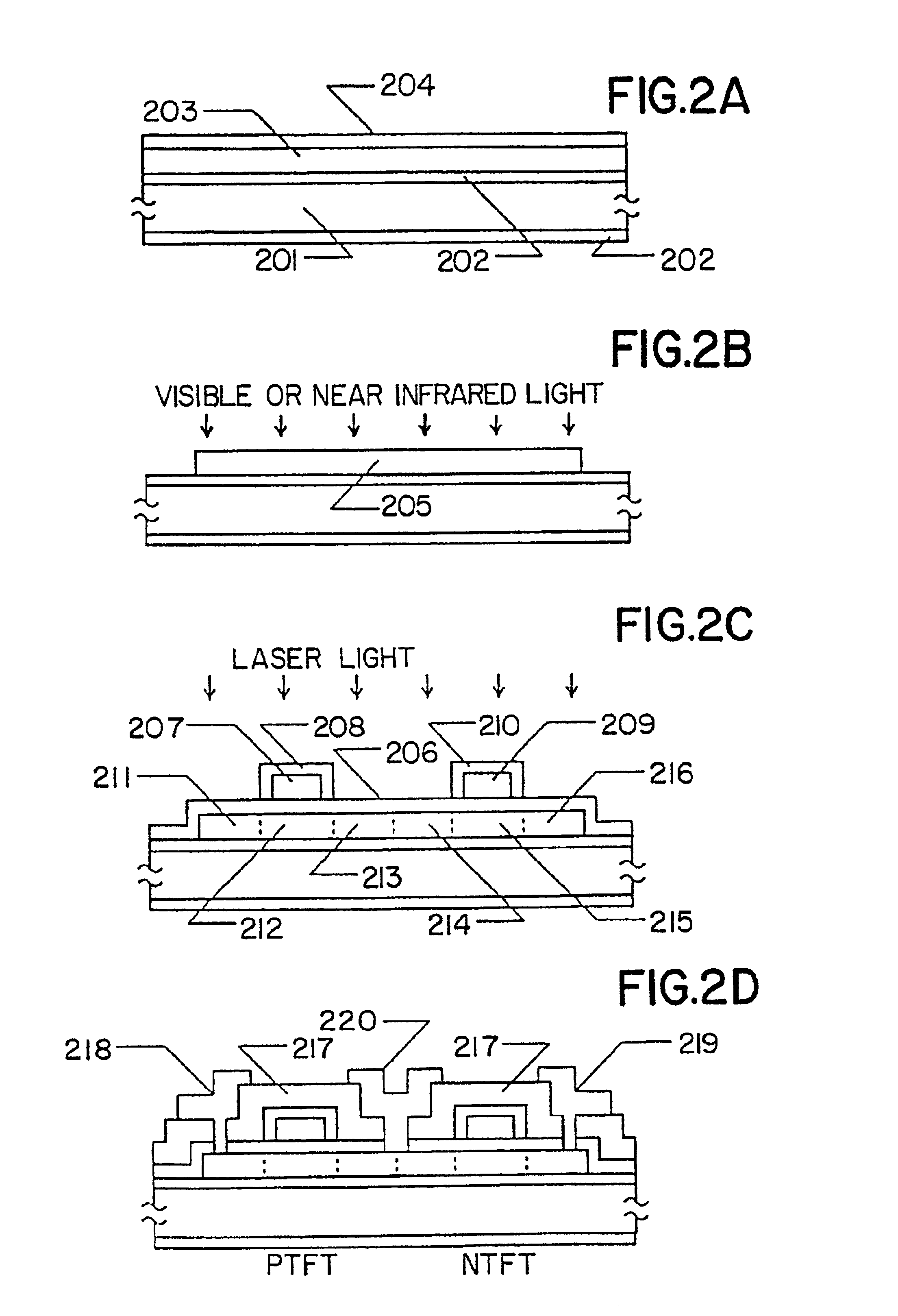
The present example is an active-matrix liquid crystal display comprising N-channel TFTs which are formed at pixels as switching devices. In the description made below, only one pixel is described but many other (generally hundreds of thousands of) pixels are formed similarly. Obviously, the TFTs are not limited to N-channel TFTs. P-channel TFTs can also be used.
The process sequence of the present example is schematically shown in FIGS. 3(A)-3(C). In the present example, Corning 7059 glass was used as a substrate 400. This substrate had a thickness of 1.1 mm and measured 300 mm by 400 mm. First, an aluminum nitride film 401 was formed to a thickness of 1000 to 5000 Å, typically 2000 Å, by sputtering or reactive sputtering techniques. Since the aluminum nitride film has a high degree of transparency and suppresses movement of ions, the film effectively prevents mobile ions from diffusing from the substrate 400 into the TFT regions. A silicon oxide film 402 was formed as a bottom film...
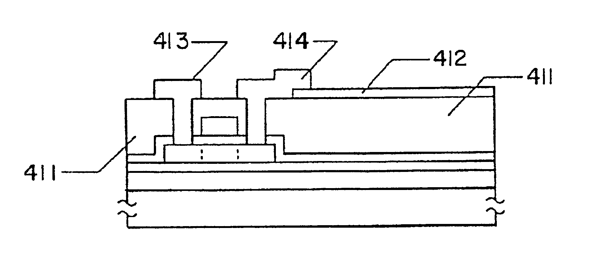
example 3
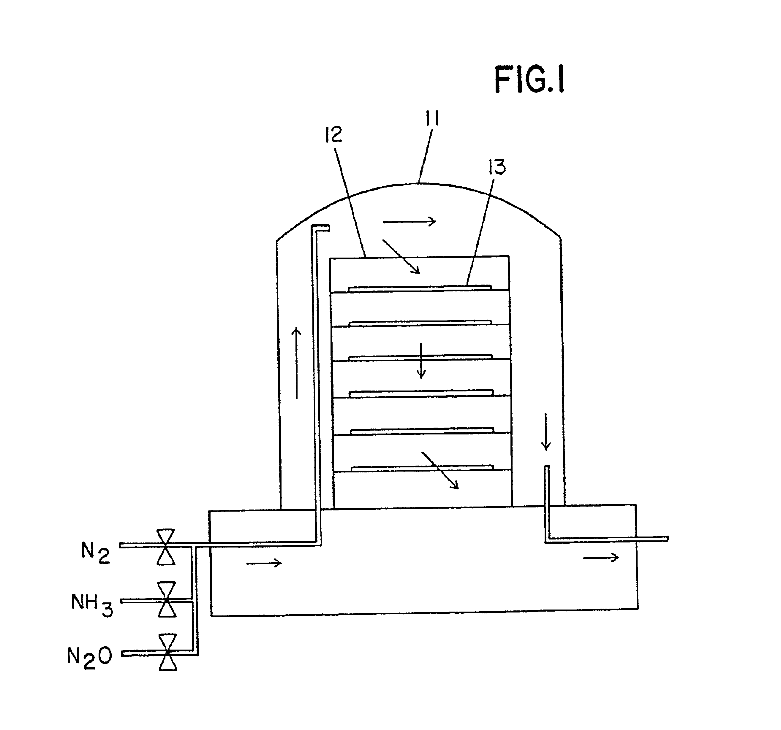
The present example is described by referring to FIGS. 4(A)-4(D). Corning 7059 glass was used as a substrate 501. An aluminum nitride film (not shown) having a thickness of 5000 Å was formed on each side of the substrate by the positive column type plasma-assisted CVD system shown in FIGS. 5 and 6. To anneal the aluminum nitride film and to prevent shrinkage, the glass substrate was previously annealed at 640° C. for 4 hours within nitrogen. Then, the substrate was slowly cooled down to 450° C. at a rate of 0.1° C. / min within nitrogen. Thereafter, the substrate was taken out of the heating furnace.
As a result of this step, the glass substrate shrank to a large extent. Shrinkage caused by a later heating step could be suppressed within 50 ppm. At the same time, the aluminum nitride (AIN) film could be annealed. Its insulation and transmissivity could be improved.
First, a bottom film 502 was formed on the substrate 501. An amorphous silicon film having a thickness of 300 to 800 Å was ...
PUM
| Property | Measurement | Unit |
|---|---|---|
| thickness | aaaaa | aaaaa |
| thickness | aaaaa | aaaaa |
| strain points | aaaaa | aaaaa |
Abstract
Description
Claims
Application Information
 - R&D Engineer
- R&D Manager
- IP Professional
- Industry Leading Data Capabilities
- Powerful AI technology
- Patent DNA Extraction
Browse by: Latest US Patents, China's latest patents, Technical Efficacy Thesaurus, Application Domain, Technology Topic, Popular Technical Reports.
© 2024 PatSnap. All rights reserved.Legal|Privacy policy|Modern Slavery Act Transparency Statement|Sitemap|About US| Contact US: help@patsnap.com