Apparatus and method for semiconductor wafer cleaning

a technology of apparatus and semiconductor wafers, applied in the direction of cleaning hollow articles, cleaning using liquids, instruments, etc., can solve the problems of failure of ic circuitry, and the need to remove particulates for proper operation, etc., to achieve significant ic test yield increase, low defect level, and small footprint

Inactive Publication Date: 2005-02-22
CASTRUCCI PAUL P
View PDF13 Cites 30 Cited by
  • Summary
  • Abstract
  • Description
  • Claims
  • Application Information

AI Technical Summary

Benefits of technology

Among the advantages of this invention may be one or more of the following. The yield enhancement system (YES) of this invention enables the production of wafers with defect levels of 0.01 defects/cm2 or less. This low defect level translates in significant IC test yield increases. Many semiconductor cleaning applications can be handled by the SCF-CT. The YES system has a significantly smaller footprint and costs less than the traditional wet-chemical process stations. The YES system of this invention is compatible with the small device dimensions and test yield requirements necessary to advance the IC fabrication process in the future. At defect densities of 0.12 defects/cm2 and lower water based wafer cleaning becomes ineffective. The YES system of this invention is a technology enabler for achieving defect densities of 0.03 defects/cm2 and lower. Furthermore, the...

Problems solved by technology

Particulate contaminants (“particulates”) frequently adhere to a surface by weak covalent bonds, electrostatic forces, van der Waals forces, hydrogen bonding, coulombic forces, or dipole-dipole interactions, making removal of the particulates difficult.
It is known that not all particulates are equally undesirable.
On the other hand, particulates that adhere to active areas or critical locations (“killer defects”) can cause failure of the IC circuitry and must be removed for ...

Method used


Image

  • Apparatus and method for semiconductor wafer cleaning
  • Apparatus and method for semiconductor wafer cleaning
  • Apparatus and method for semiconductor wafer cleaning

Examples


Embodiment Construction

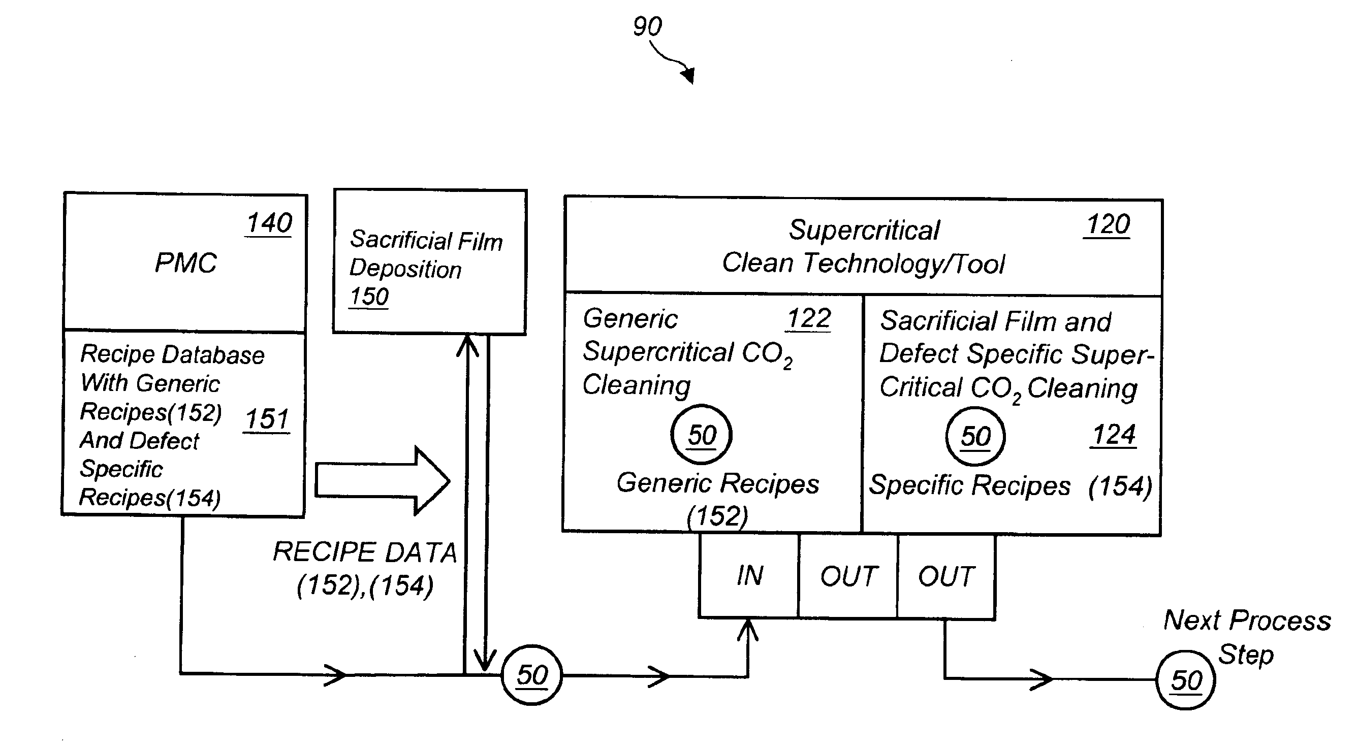
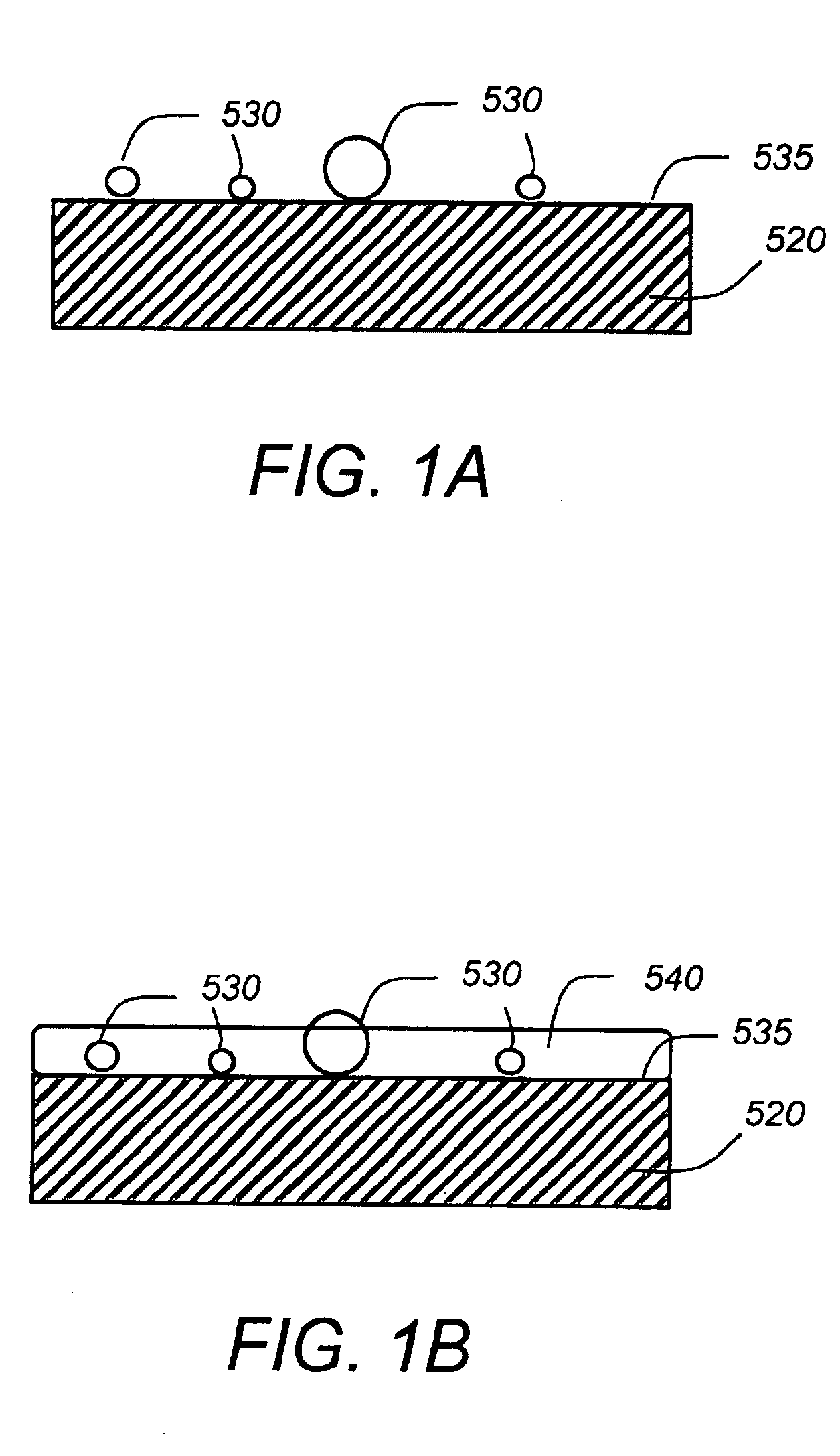
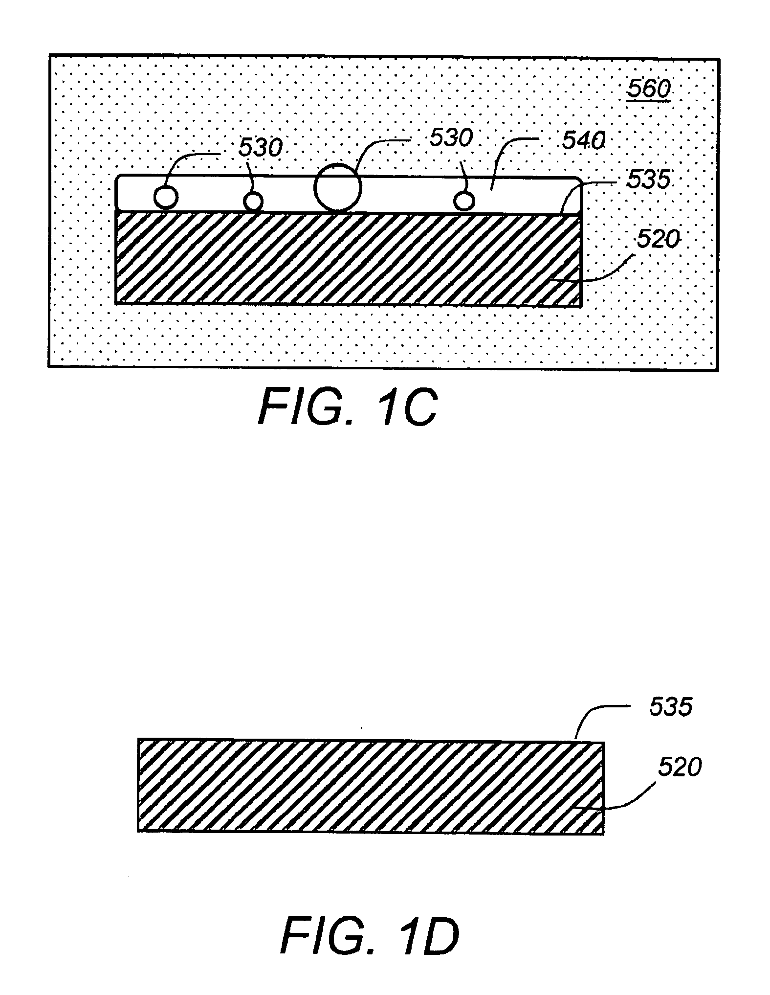
Referring to FIGS. 1A-1D, a substrate 520 (having a surface 535) initially has particulate contaminants 530 of various sizes adherent to surface 535. A sacrificial film 540 is applied to surface 35. The solvent is evaporated, leaving a dry film (FIG. 1B). Substrate 520 with its contaminant particles 530 and sacrificial film 540 is placed in a supercritical. cleaning chamber 560 where at temperatures above 31° C. and pressure of 1072 psi, the liquid and gaseous phases of CO2 combine to form supercritical CO2 (SCCO2). Sacrificial film 540 and the particulate contaminants solvate within the SCCO2 and are evacuated into a low pressure chamber, where they become insoluble and are precipitated from the liquid CO2. The surface 535 is scanned for particles 530 remaining on surface 535 and the locations of stubborn particulate defects, if any, are recorded in a data file. The surface scanning may be performed by utilizing a scanning electron microscope—defect review tool 215 (SEM-DRT describ...


PUM

PropertyMeasurementUnit
Temperatureaaaaaaaaaa
Fractionaaaaaaaaaa
Pressureaaaaaaaaaa

Abstract

An improved method for removing contaminant particles from a surface of a semiconductor wafer includes forming a sacrificial film on the surface of the wafer and then removing the sacrificial film by supercritical fluid cleaning. The removal of the sacrificial film via the supercritical fluid cleaning process facilitates removing the contaminant particles. The method further includes identifying and characterizing the contaminant particles and creating a record of the contaminant particle data. The composition of the sacrificial film is selected based on the contaminant particles data and the supercritical cleaning recipe is selected based on the composition of the sacrificial film and the contaminant particles data.

Description

FIELD OF THE INVENTIONThe present invention relates to an apparatus and a method for cleaning semiconductor wafers, and more particularly to semiconductor wafer cleaning that integrates a defect detection and characterization system, and a defect removal system using a sacrificial film and supercritical cleaning.BACKGROUND OF THE INVENTIONSurface cleaning of a semiconductor wafer has a significant bearing on device test yields. As the semiconductor industry pushes for smaller integrated circuit (IC) dimensions, e.g., 0.35 micron, 0.25 micron and 0.1 micron, the defect density level and size of the smallest particle capable of causing a failure in an IC decrease, as well. For example, for IC devices of 0.35 microns or less particles of the order of one third of the device size, i.e., 0.12 micron or less can cause the circuit to malfunction. Moore's Law projects that by 2005 IC devices will have over 700 million transistors per chip. The Semiconductor Industry Association (SIA) Roadma...

Claims


Application Information

Patent Timeline
IPC IPC(8): B08B7/00H01L21/02H01L21/306G01Q60/00
CPCB08B7/0021H01L21/02063H01L21/02043Y10S134/902
Inventor CASTRUCCI, PAUL P.
Owner CASTRUCCI PAUL P
Why Eureka
Try Eureka