Optically scanning apparatus and defect inspection system

Inactive Publication Date: 2005-02-22
LASERTEC CORP
View PDF6 Cites 63 Cited by
  • Summary
  • Abstract
  • Description
  • Claims
  • Application Information

AI Technical Summary

Benefits of technology

An object of the present invention is to provide an optically scanning apparatus and defect

Problems solved by technology

The surface of a semiconductor wafer, however, has micro step differences or unevenness of an atomic level, so the intensity of the light scattered from the surface of a normal sample is too strong and scattered light due to defects present on the surface of the sample is difficult to differentiated from the light scattered from a normal surface.
As a result, the resolution of detection of d

Method used


Image

  • Optically scanning apparatus and defect inspection system
  • Optically scanning apparatus and defect inspection system
  • Optically scanning apparatus and defect inspection system

Examples


Embodiment Construction

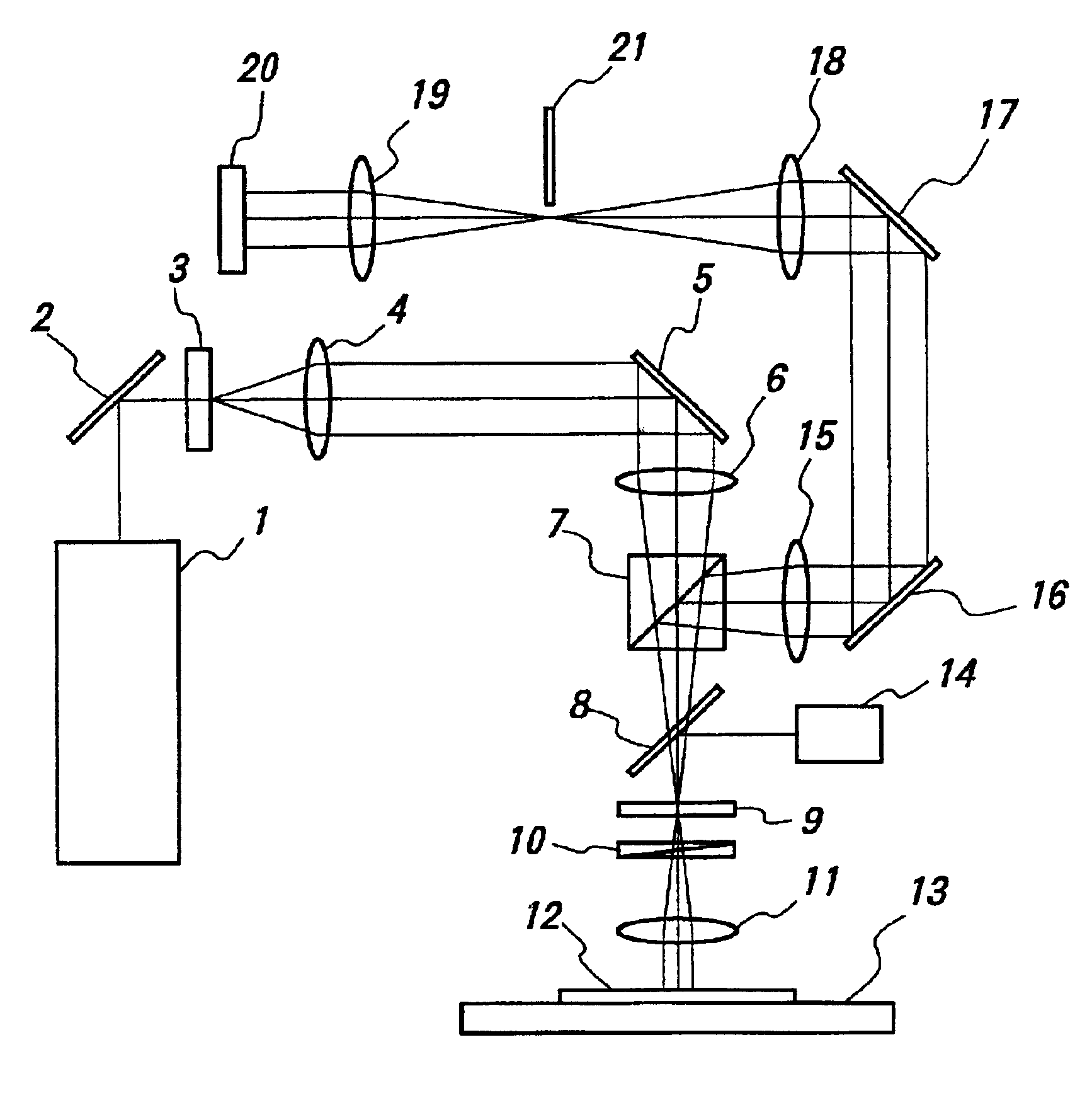
Preferred embodiments of the present invention will be described in detail below while referring to the attached figures.

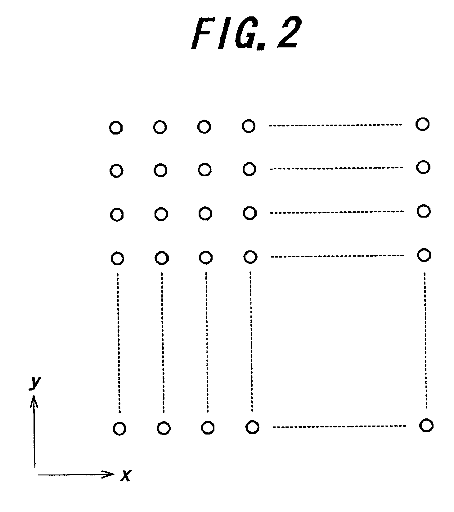
FIG. 1 is a schematic view showing an embodiment of an optically scanning apparatus according to the present invention. In this example, as a light source 1, use is made of a YAG laser generating laser light of a wavelength of for example 532 nm. The beam emitted from the laser source 1 is reflected by a full reflection mirror 2 and strikes a diffraction grating 3. The diffraction grating 3 is comprised of a two-dimensional diffraction grating. The striking light beam is converted to a two-dimensional beam array of m×n number of light beams (m and n being natural numbers of 2 or more). In this example, a single light beam is used to generate a 33×33 two-dimensional beam array. FIG. 2 is a view of the converted beam array projected on a plane perpendicularly intersecting the light axis. The m×n number of light beams form a two-dimensional beam array comprised of li...


PUM


Abstract

An optically scanning apparatus and defect inspection system able to detect a defect with a high resolution and able to greatly shorten the inspection time. An radiation beam generated from a light source is converted to a light beam array of an m×n matrix by a two-dimensional diffraction grating. The light beams of the light beam array are focused into micro spots by an objective lens and projected on a sample. Therefore, a two-dimensional light spot array of an m×n matrix is formed on a sample. The sample stage rotates and moves rectilinearly in an r direction, so the sample surface is scanned by the m×n matrix of light spots. As a result, the sample surface is spirally scanned by a light beam of a belt shape of the scan width, so can be scanned at a high speed. Further, the beams reflected by the sample surface are received by light receiving elements separated by light blocking members, so a confocal optical system is formed and as a result the resolution of detection of defects becomes much higher.

Description

BACKGROUND OF THE INVENTION1. Field of the InventionThe present invention relates to an optically scanning apparatus for optically scanning the surface of a sample by m×n (m and n being natural numbers of 2 or more) number of sub beams and a defect inspection system for detecting a defect existing on the surface of a sample using this optically scanning apparatus.2. Description of the Related ArtAlong with the increasing miniaturization of LSIs (large scale integrations), there has been strong demand for development of a defect inspection system able to accurately detect micro defects existing on the surface of a semiconductor wafer, patterned wafer, mask blank, etc. In particular, there has been strong demand for development of a defect inspection system able to accurately detect micro defects since the manufacturing yield falls by a large margin when defects are present on a semiconductor wafer before processing for fabrication of semiconductor devices.In the past, as a system for...

Claims


Application Information

Patent Timeline
IPC IPC(8): G01N21/88G01N21/89G01B11/30G01N21/956
CPCG01N21/8901
Inventor KUSUNOSE, HARUHIKO
Owner LASERTEC CORP
Why Eureka
Try Eureka