

Semiconductor device and method for manufacturing the same
a technology of semiconductors and semiconductors, applied in the field of semiconductors, can solve the problems of low effect of blocking impurity ions, varying the electric characteristics of tft, and internal stress, and achieve the effect of reducing internal stress and improving tft reliability
- Summary
- Abstract
- Description
- Claims
- Application Information
AI Technical Summary
Benefits of technology
Problems solved by technology
Method used
Image

Examples
embodiment 1
[0050]Preferred Embodiment 1
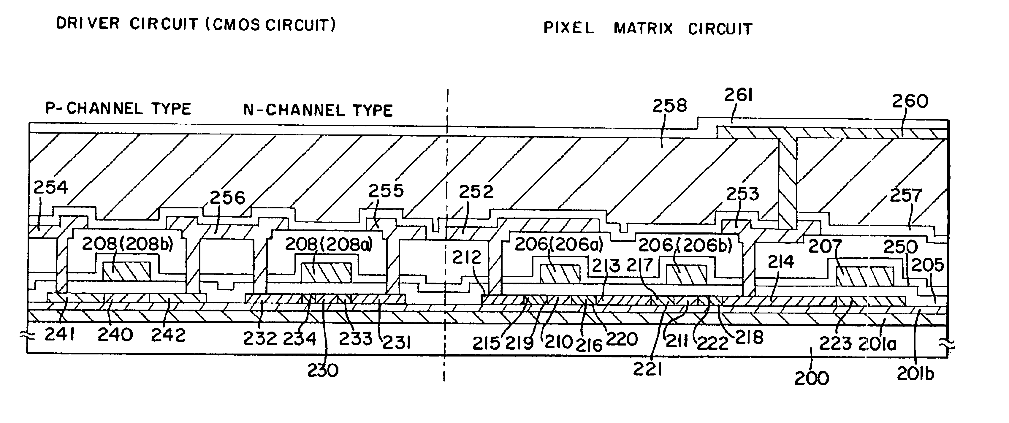
[0051]In the present preferred embodiment, a manufacturing process of a CMOS circuit including an n-channel-type TFT and a p-channel-type TFT will be described. A preferred embodiment will be described in which an insulating film in accordance with the present invention is used for a top-gate-type underlying film. Also, a process to the present invention will be described.
[0052]A manufacturing process of the present preferred embodiment will be described below with reference to FIG. 1 and FIG. 2. Also, in the present preferred embodiment, four conditions were set and the composition of the underlying film suitable for preventing the deterioration of a TFT was investigated.
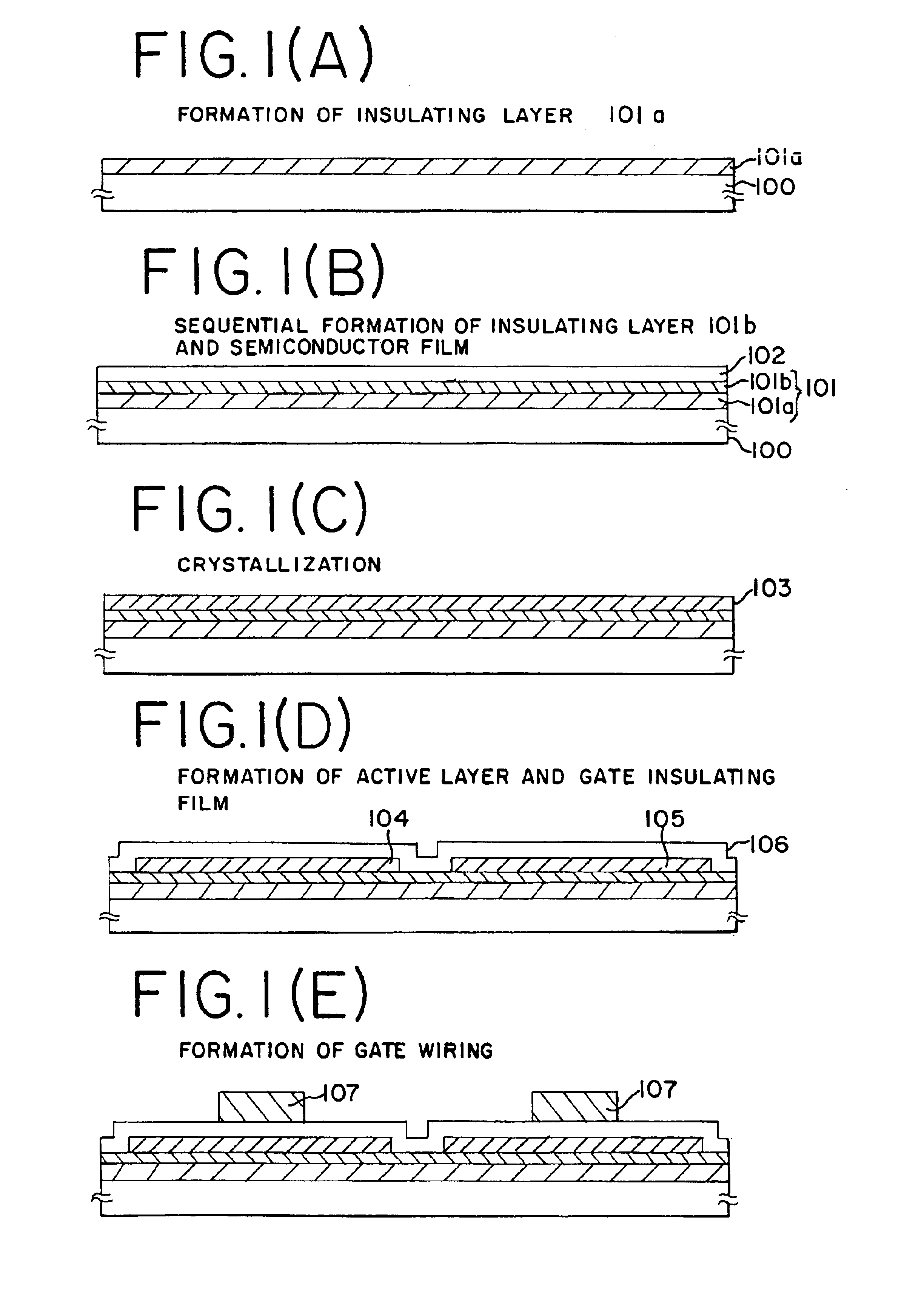
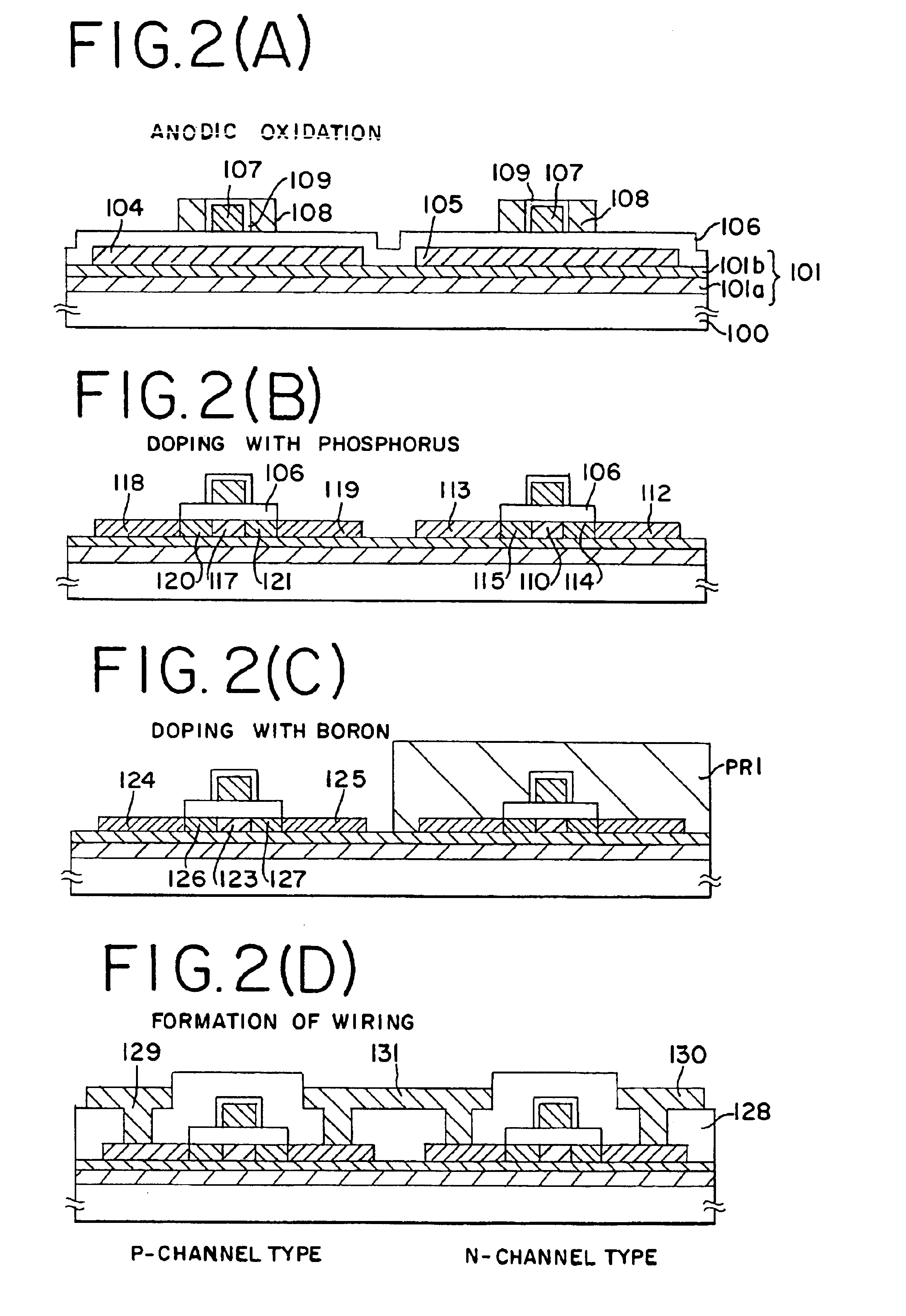
[0053](Process for Forming an Underlying Film / A Semiconductor)
[0054]A 5-inch 1737 glass substrate (made by Corning Corp.) was used as a glass substrate 100. An underlying film 101 was formed in contact with the whole surface of the glass substrate 100. The underlying film 101 was made of...
embodiment 2
[0112]Preferred Embodiment 2
[0113]While the insulating layer 101b containing Si and O was formed of the silicon oxide film using TEOS and O2 in the preferred embodiment 1, it can be formed of a silicon oxide nitride film. In this case, the silicon oxide nitride film may be formed using SiH4 and N2O as the raw material gases.
[0114]For example, it is recommended that the silicon oxide nitride film be formed as the underlying insulating layer 101a under the same conditions as is used for the insulating layer 101a of the substrate-3, and that the silicon oxide nitride film be formed as the insulating layer 101b under the same conditions as is used for the insulating layer 101b of the substrate-1.
[0115]The insulating layer 101a made of silicon oxide nitride was formed in a film thickness of 100 nm and the insulating layer 101b made of silicon oxide nitride was formed in a film thickness of 200 nm. There was no problem in a dielectric property. The insulating film made of this laminated f...
embodiment 3
[0183
[0184]In the present embodiment, an example of a pixel structure applicable to the pixel part of an EL display device shown in an embodiment 10 will be shown in FIG. 13(A) to (C). In this connection, in the present embodiment, a reference numeral 3401 designates the source wiring of a switching TFT 3402, a reference numeral 3403 designates the gate wiring of a switching TFT 3402, a reference numeral 3404 designates a current control TFT, a reference numeral 3405 designates a condenser, reference numerals 3406 and 3408 designate current supply wirings, and a reference numeral designates 3407 designates an EL element.
[0185]FIG. 13(A) is an example in the case where the current supply wiring 3406 is common to two pixels. In other words, this example is characterized in that two pixels are formed symmetrically with respect to a line of the current supply wiring 3406. In this case, the number of current supply wirings can be reduced and hence the pixel part can be made in higher def...
PUM
 Abstract
Description
Claims
Application Information