
Chemical/mechanical polishing slurry and chemical mechanical polishing method using the same

a technology of mechanical polishing and slurry, which is applied in the direction of lapping machines, other chemical processes, polishing compositions, etc., can solve the problems of uneven wafer surface, excessive polishing of polishing stoppers, poor selectivity, etc., and achieves effective passivation of polishing stoppers, high selectivity, and rapid removal of target layers

Inactive Publication Date: 2005-03-08
SAMSUNG ELECTRONICS CO LTD
View PDF7 Cites 30 Cited by
  • Summary
  • Abstract
  • Description
  • Claims
  • Application Information

AI Technical Summary

Benefits of technology

The present invention is about methods for making CMP slurries with high selectivity. The slurry can quickly remove a target layer while effectively passivating a polishing stopper, with a high selectivity of about 30:1 to about 50:1. The slurry comprises metal oxide abrasive particles, a removal rate accelerator, an anionic polymeric passivation agent, a C1-C12 anionic passivation agent, and water. The slurry can also contain a pH controller and a pH in a range of about 3 to about 6. The invention also includes a CMP process using the CMP slurry on a target layer on a surface of a wafer.

Problems solved by technology

However, with conventional CMP slurries, which are used in the formation of shallow trench isolation (STI) or the formation of an interlayer dielectric (ILD) layer, wherein a self-aligned contact hole exposing a source / drain region of a DRAM is formed, the selectivity of a target layer to be polished (e.g., an oxide layer) with respect to a polishing stopper (e.g., a silicon nitride layer) is at a ratio of 4:1, which is considered poor selectivity.
As a result, the polishing stopper is excessively polished.
Further, with conventional slurries, the polishing stopper remaining after the CMP has thickness variations, which results in an uneven wafer surface and reduces a margin for subsequent device manufacturing processes.
As a result, the characteristics of the semiconductor device can degrade.

Method used


Image

  • Chemical/mechanical polishing slurry and chemical mechanical polishing method using the same
  • Chemical/mechanical polishing slurry and chemical mechanical polishing method using the same
  • Chemical/mechanical polishing slurry and chemical mechanical polishing method using the same

Examples


experimental example 1

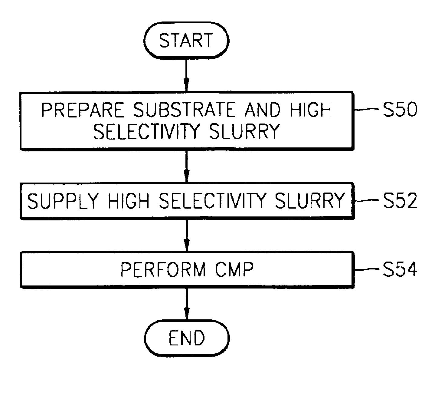
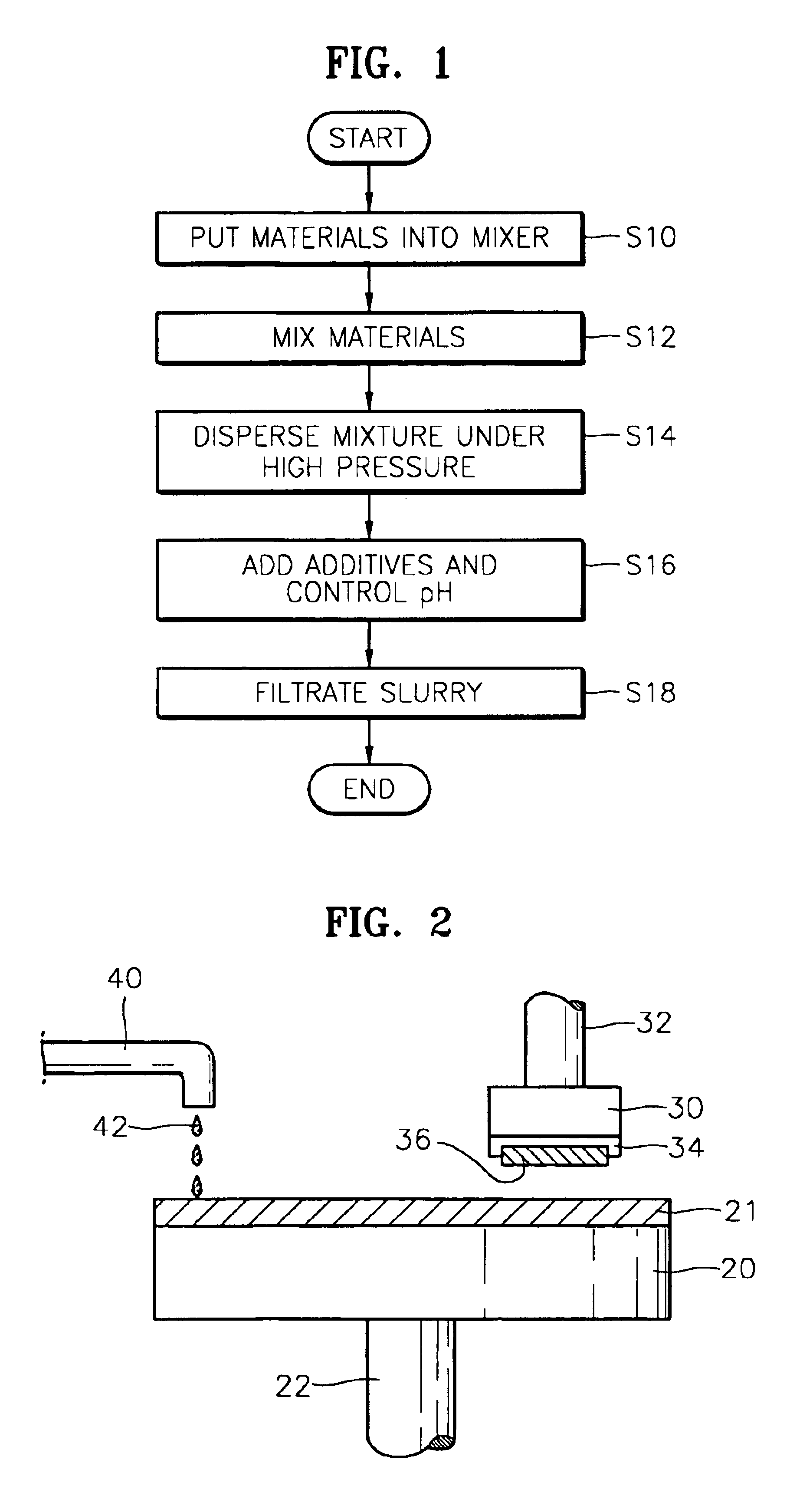
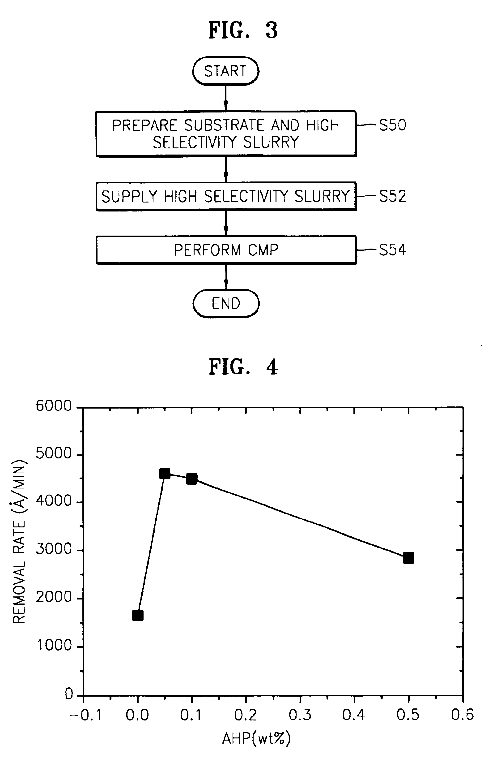
In this experiment, based on the method described with respect to FIG. 1, various slurries were prepared by adding ammonium hydrogen phosphate (AHP) as a removal rate accelerator in different amounts to an aqueous solution containing 1 wt % ceria (metal oxide abrasive particles) as a first additive.

PE-TEOS blanket wafers, each having an 8000 Å—thick oxide (PE-TEOS) layer, were prepared as sample wafers.

CMP was then performed on the sample wafers while supplying the slurries containing different amounts of AHP (as shown in Table 1) thereon, and oxide removal rates were measured. The CMP was performed using MIRRA_MESA equipment (RODEL Co., Ltd) under the following conditions: an IC1000 stack pad at a membrane force of 3.5 psi, a retaining ring force of 4.5 psi, an inner tube force of 3.5 psi, a table speed of 110 rpm, a head speed of 104 rpm, and a slurry flow rate of 3000 mL / min. The CMP results are shown in Table 1. FIG. 4 is a graphical illustration of the results.

TABLE 1AHP, wt %O...

experimental example 2

In this experiment, various slurries were prepared by adding 0.25 wt % AHP and different amounts of poly(methacrylic acid) (PMA) as an anionic polymeric passivation agent to an aqueous solution of 1 wt % ceria.

PE-TEOS and silicon nitride (Si3N4) blanket wafers, wherein an oxide (PE-TEOS) layer and a silicon nitride layer were deposited to thicknesses of 8000 Å and 2000 Å, respectively, were prepared as sample wafers.

CMP was performed on the sample wafers while supplying the slurries prepared with the compositions of Table 2, using the same CMP apparatus and under the same operating conditions as in Experimental Example 1. Oxide and silicon nitride removal rates and selectivity were measured during the CMP. The results are shown in Table 2 below. FIG. 5 is a graphical illustration of the results.

TABLE 2Removal rate, Å / minAHP,OxideSilicon nitridewt %PMA, wt %pH(PE-TEOS)(Si3N4)Selectivity0.250.055399310783.7:10.250.1537069753.8:10.250.5524486793.6:10.251516174783.4:1

As can be gleaned f...

experimental example 3

In this experiment, various slurries were prepared by adding 0.2 wt % AHP and different amounts of potassium hydrogen phthalate (PHP) as a C1-C12 anionic passivation agent to an aqueous solution of 1 wt % ceria.

The same sample wafers as in Experimental Example 2 were prepared, and CMP was performed in the same CMP apparatus and under the same operating conditions as in Experimental Example 2. Oxide and silicon nitride removal rates and selectivity were measured during the CMP. The results are shown in Table 3 below. FIG. 6 is a graphical illustration of the results.

TABLE 3Removal rate, Å / minAHP,OxideSilicon nitridewt %PHP, wt %pH(PE-TEOS)(Si3N4)Selectivity00512425422.3:10.205266812062.2:10.20.015261511552.3:10.20.1526688993.0:10.20.25527447723.6:1

As can be gleaned from Table 3 and FIG. 6, as the amount of PHP used as the C1-C12 anionic passivation agent increases, the silicon nitride removal rate decreases. The passivation effect of the anionic passivation agent is evident. Also, in...


PUM

PropertyMeasurementUnit
pressureaaaaaaaaaa
flow rateaaaaaaaaaa
pHaaaaaaaaaa

Abstract

CMP (chemical / mechanical polishing) slurries that can rapidly remove a target layer and can effectively passivate a polishing stopper, with high selectivity. In one aspect, a CMP slurry comprises metal oxide abrasive particles, a removal rate accelerator, an anionic polymeric passivation agent having a molecular weight in a range of about 1,000 to about 100,000, a C1-C12 anionic passivation agent, and water.

Description

CROSS-REFERENCE TO RELATED APPLICATIONThis application claims priority to Korean Patent Application No. 2002-48403 filed on Aug. 16, 2002, which is fully incorporated herein by reference.TECHNICAL FIELD OF THE INVENTIONThe present invention generally relates to CMP (chemical / mechanical polishing) slurries for use in the manufacture of microelectronic devices. More particularly, the present invention relates to CMP slurries that can rapidly remove a target layer and effectively passivate a polishing stopper, with high selectivity.BACKGROUNDSemiconductor devices have become increasingly more integrated and smaller with multilayered interconnections and consequently, the amount of processing steps have increased to form multiple conductive layers or insulating layers on a wafer. To eliminate steps in semiconductor device fabrication, CMP, which is a combination of chemical and mechanical processes, is commonly used. CMP was developed in the late 1980s by International Business Machines...

Claims


Application Information

Patent Timeline
Patent Type & Authority Patents(United States)
IPC IPC(8): C09G1/00C09G1/02H01L21/02H01L21/3105B24B37/00C09K3/14H01L21/302H01L21/304H01L21/3205H01L21/321H01L21/768
CPCH01L21/31053C09G1/02H01L21/302
Inventor LEE, JONG-WONHONG, CHANG-KILEE, JAE-DONG
Owner SAMSUNG ELECTRONICS CO LTD
Learn More