Method of depositing transition metal nitride thin films

a technology of transition metal nitride and thin film, which is applied in the direction of crystal growth process, chemical vapor deposition coating, coating, etc., can solve the problems of affecting the electrical properties of the circuit, and copper is prone to diffusion to the surrounding materials, etc., to achieve low resistivity, easy to handle, and acceptable growth rate of the film

Inactive Publication Date: 2005-03-08
ASM INTERNATIONAL
View PDF12 Cites 80 Cited by
  • Summary
  • Abstract
  • Description
  • Claims
  • Application Information

AI Technical Summary

Benefits of technology

The invention is based on the surprising finding that by feeding into a reactor chamber, which contains a substrate, a suitable transition metal compound and, a reducing boron compound pulse and a nitrogen compound, a metal nitride film with low resistivity can be grown. According to the present invention, the reaction between the gaseous boron compound and the metal species reduces the metal compound and gives rise to gaseous reaction byproducts, which easily can be removed from the reaction space.
According to a preferred embodiment of the invention, the metal nitride thin films are grown by an ALD type process. This is carried out by sequentially feeding into a reactor chamber, which contains a substrate, alternate pulses of a suitable transition metal compound, a reducing boron compound pulse and a nitrogen compound, said boron compound and said nitrogen compound being fed after the metal compound. Thus, a metal nitride film with low resistivity can be grown in accordance with the principles of ALD method. According to the present invention, the reaction between the gaseous boron compound and the metal species bound to the surface reduces the metal compound and gives rise to gaseous reaction byproducts, which easily can be removed from the reaction space.
A number of considerable advantages are achieved with the aid of the present invention Metal nitride thin films, in particular tungsten nitride thin films, can be grown at low temperatures. The boron compounds used as source materials are easy to handle and vaporise.
As mentioned above, the boron compounds formed as byproducts of the reaction between the metal species and the reducing boron compound are essentially gaseous and they exit the reactor easily when purging with an inert gas. The boron residues in the film are on a very low level, typically below 5 wt-%, preferably 1 wt-% or less and in particular 0.5 wt-% or less. The resistivity of the film is low. The growing rate of the film is acceptable. Also the reaction times are short, and in all it can be said that films can be grown very effectively by means of the present process.
The film grown with the present process exhibits good thin films properties. Thus, especially the metal nitride films obtained by an ALD type process have an excellent conformality even on uneven surfaces and on trenches and vias. The method also provides an excellent and automatic self-control for the film growth.
The metal nitride thin films grown by the present invention can be used, for example, as ion diffusion barrier layers in integrated circuits. Tungsten nitride stops effectively oxygen and increases the stability of metal oxide capacitors. Transition metal nitrides and especially tungsten nitride is also suitable as an adhesion layer for a metal, as a thin film resistor, for stopping the migration of tin through via holes and improving the high-temperature processing of integrated circuits.

Problems solved by technology

Especially copper is prone to diffusion to the surrounding materials.
Diffusion affects the electrical properties of the circuits and active components may malfunction.
There are, however, drawbacks related to these prior art methods.
Traditional CVD processes may leave significant amounts of impurities in thin films, especially at low deposition temperatures.

Method used


Image

  • Method of depositing transition metal nitride thin films
  • Method of depositing transition metal nitride thin films

Examples


example 1

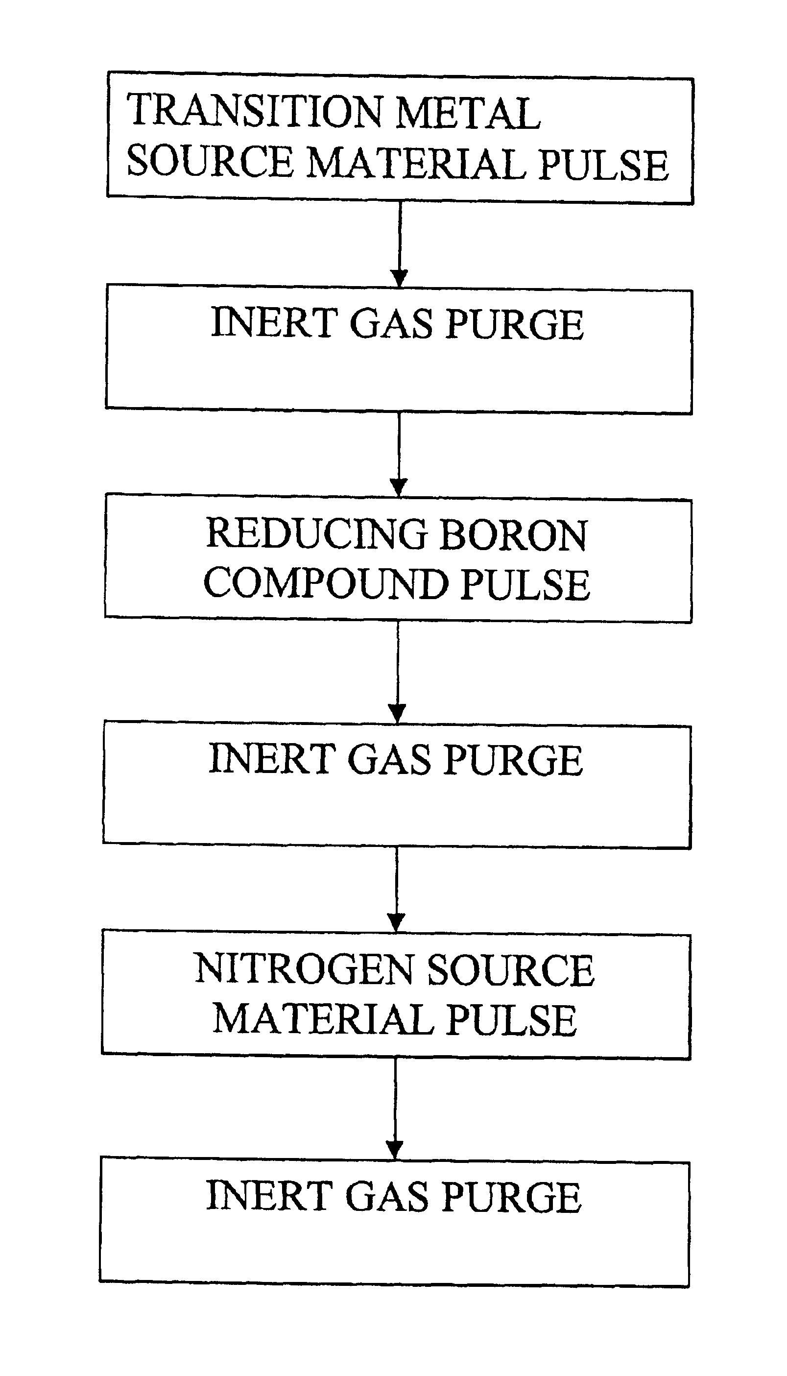
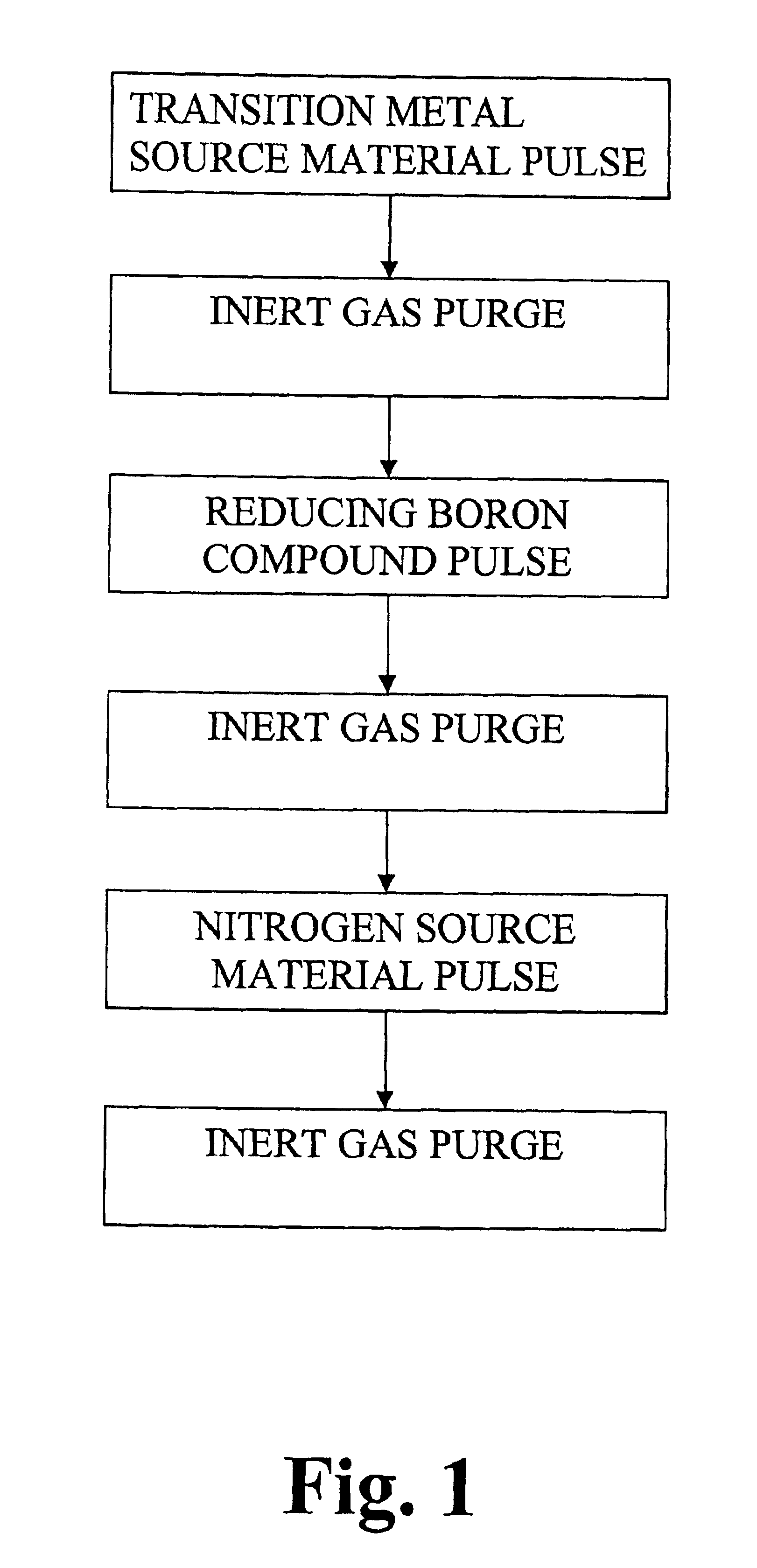
Tungsten hexafluoride (WF6) and ammonia (NH3) were used as source chemicals. Both chemicals are liquefied gases at room temperature and posses high enough vapor pressure without additional heating for the ALD process. Source tubing and the reactor were purged with nitrogen gas which had a purity of 99.9999% (i.e. 6.0). The N2 gas was prepared from liquid nitrogen. A 200-mm silicon wafer was loaded to an ALD reactor as described in Finnish Patent No. 100409 of assignee. Source chemicals were pulsed alternately to the substrates at the reaction chamber. The deposition was started and ended with an NH3 pulse. The pulsing cycle consisted of the following steps:NH3 vapor pulse 0.5 sN2 gas purge 1.0 sWF6 vapor pulse 0.25 sN2 purge 0.8 s

The pulsing cycle was repeated for 500 times which produced a 30 nm film with the typical growth rate of 0.6 Å / cycle. The composition, impurities and the thickness of the resulting thin film were analyzed by Electron Diffraction Spectroscopy (referred to as...

example 2

Tungsten hexafluoride (WF6), triethylboron (CH3CH2)3B and ammonia (NH3) were used as source chemicals. All the chemicals are liquids or liquefied gases at room temperature and poses high enough source vapor pressure without additional heating for the ALD process. Source tubing and the reactor were purged with nitrogen gas which had a purity of 99.9999% (i.e. 6.0). The N2 gas was prepared from liquid nitrogen. A 200-mm silicon wafer was loaded to an F200 ALD reactor. Source chemicals were pulses alternately to the substrates at the reaction chamber. The pulsing cycle consisted of the following steps:WF6 vapor pulse 0.25 sN2 purge 0.8 s(CH3CH2)3B vapor pulse 0.01 sN2 gas purge 0.5 sNH3 vapor pulse 0.25 sN2 gas purge 0.5 s

The pulsing cycle was repeated for 500 times resulting in a 30-nm film at 360° C. The samples were analyzed by EDS for thickness and composition. The thin film consisted of tungsten and nitrogen while boron could not be seen in detectable amounts. There was 3 wt.-% of...


PUM

PropertyMeasurementUnit
feature sizesaaaaaaaaaa
thicknessaaaaaaaaaa
pressureaaaaaaaaaa

Abstract

This invention concerns a method for depositing transition metal nitride thin films by an Atomic Layer Deposition (ALD) type process. According to the method vapor-phase pulse of a source material, a reducing agent capable of reducing metal source material, and a nitrogen source material capable of reacting with the reduced metal source material are alternately and sequentially fed into a reaction space and contacted with the substrate. According to the invention as the reducing agent is used a boron compound which is capable of forming gaseous reaction byproducts when reacting with the metal source material.

Description

BACKGROUND OF THE INVENTION1. Field of the InventionThe present invention relates to metal nitride thin films. In particular, the invention concerns a method of growing tungsten nitride thin films by Atomic Layer Deposition (referred to as ALD hereinafter).2. Description of Related ArtThe integration level of components in integrated circuits is increasing, which rapidly brings about a need for a decrease of the size of components and interconnects. Design 15 rules are setting the feature sizes to ≦0.2 μm. Complete film coverage on deep bottoms and vias is bard to obtain.Integrated circuits contain interconnects which are usually made of aluminium or copper. Especially copper is prone to diffusion to the surrounding materials. Diffusion affects the electrical properties of the circuits and active components may malfunction. The diffusion of metals from interconnects into active parts of the device is prevented with an electrically conductive diffusion barrier layer. Favored diffusio...

Claims


Application Information

Patent Timeline
Patent Type & Authority Patents(United States)
IPC IPC(8): C30B29/36C30B29/10C30B29/38C23C16/32C30B25/02C30B29/02C23C16/44C23C16/34H01L21/285H01L21/70H01L21/02H01L21/768C23C16/455
CPCC23C16/32C23C16/34H01L21/76843H01L21/28562C30B29/38C30B29/36C30B29/02C23C16/44C23C16/4401C23C16/45531C23C16/45534C30B25/02H01L21/76856
Inventor ELERS, KAI-ERIKHAUKKA, SUVI PAIVIKKISAANILA, VILLE ANTEROKAIPIO, SARI JOHANNASOININEN, PEKKA JUHA
Owner ASM INTERNATIONAL
Why Eureka
Try Eureka