Semiconductor integrated circuit device and the process of manufacturing the same for reducing the size of a memory cell by making the width of a bit line than a predetermined minimum size

a technology of integrated circuit and memory cell, which is applied in the direction of semiconductor devices, electrical devices, transistors, etc., can solve the problems of increasing the parasitic capacitance difficult to ensure, short circuit, etc., and achieves the reduction of the stability of the bit line, the effect of high accuracy and reduced photoresist film siz

Inactive Publication Date: 2005-03-15
LONGITUDE LICENSING LTD
View PDF13 Cites 12 Cited by
  • Summary
  • Abstract
  • Description
  • Claims
  • Application Information

AI Technical Summary

Benefits of technology

[0012]However, the above-mentioned method of making the width of the photoresist film fine by etching it in an anisotropic manner presents some difficulty in controlling the amount of etching of the photoresist film with high accuracy, and hence it presents a problem in that the stability in size of the photoresist film is reduced after it is etched. Also, in the case where the metal film is patterned by using the photoresist film having a width finer than the minimum width determined by the limit of resolution of the photolithography, another problem is also presented in that a variation in the amount of etching of the photoresist film increases and the stability in size of the bit line is reduced.
[0013]Further, in the case where the photoresist film applied on top of the metal film is finely patterned, still another problem is presented in that a variation in the size of the photoresist caused by halation or the like becomes apparent. Also, when a reflection preventing film or the like is formed on the film underlying the photoresist film as a countermeasure against this problem, a further problem is presented in that the controllability of etching is reduced.
[0014]Also, in the manufacturing process of the DRAM having the above-mentioned COB structure, in order to form the capacitance element for storing information on top of the bit line with good yield, it is necessary to deposit a silicon oxide film (a second silicon oxide film) in the gap between the bit lines and on top of the bit line and then to planarize the surface of the silicon oxide film using a CMP method. For this reason, in order to ensure a polishing margin, it is necessary to leave the silicon oxide film to some extent of thickness on top of the bit line, which results in an increase the level of the region where the memory cell is formed (memory array). As a result, this increases the aspect ratio of a connection hole for connecting an Al wiring formed on top of the capacitance element for storing information to the MISFET of the peripheral circuit and hence reduces the manufacturing yield of the connection hole and the reliability in connection of a conductive layer buried in the connection hole.
[0015]It is an object of the present invention to provide a technology for reducing the size of a memory cell of a DRAM by making the width of a bit line finer than the minimum size determined by the limit of resolution of photolithography.
[0016]It is another object of the present invention to provide a technology for improving the detection sensitivity of a signal stored in a capacitance for storing information by reducing the capacitance parasitic on the bit line.
[0017]It is still another object of the present invention to provide a technology for improving the manufacturing yield of a DRAM by reducing the height of a memory array.

Problems solved by technology

Accordingly, if the pitch of the bit line is reduced in a DRAM having the COB structure to reduce the size of a memory cell, it is difficult to ensure an alignment allowance between the bit line and the through hole passing the gap between the bit lines, which in turn will present a problem in that a plug buried in the through hole and the bit line may create a short circuit.
However, in the case where the self-alignment contact (SAC) technology is adopted in which the surrounding area of the bit line is covered with the silicon nitride film, the dielectric constant of silicon nitride is more than two times that of silicon oxide and hence increases the parasitic capacitance of the bit line, which in turn presents another problem in that it becomes difficult to detect a signal stored in the capacitance element for storing information.

Method used


Image

  • Semiconductor integrated circuit device and the process of manufacturing the same for reducing the size of a memory cell by making the width of a bit line than a predetermined minimum size
  • Semiconductor integrated circuit device and the process of manufacturing the same for reducing the size of a memory cell by making the width of a bit line than a predetermined minimum size
  • Semiconductor integrated circuit device and the process of manufacturing the same for reducing the size of a memory cell by making the width of a bit line than a predetermined minimum size

Examples


embodiment 2

4]FIG. 29(A) through FIG. 29(D) are cross-sectional views showing a step of the method of manufacturing a DRAM of embodiment 2 as seen along lines A-A′; B-B′; C-C′ and D-D′; respectively, in FIG. 1.

[0085]FIG. 30(A) through FIG. 30(D) are cross-sectional views showing a step of the method of manufacturing a DRAM of embodiment 2 as seen along lines A-A′; B-B′; C-C′ and D-D′; respectively, in FIG. 1.

[0086]FIG. 31(A) through FIG. 31(D) are cross-sectional views showing a step of the method of manufacturing a DRAM of embodiment 2 as seen along lines A-A′; B-B′; C-C′ and D-D′, respectively, in FIG. 1.

embodiment 3

[0087]FIGS. 32(A) and 32(B) are cross-sectional views showing a step of the method of manufacturing a DRAM of embodiment 3 in accordance with the present invention.

[0088]FIGS. 33(A) and 33(B) are cross-sectional views showing a step of the method of manufacturing a DRAM of embodiment 3 in accordance with the present invention.

[0089]FIGS. 34(A) and 34(B) are cross-sectional views showing a step of the method of manufacturing a DRAM of embodiment 3 in accordance with the present invention.

[0090]FIGS. 35(A) and 35(B) are cross-sectional views showing a step of the method of manufacturing a DRAM of embodiment 3 in accordance with the present invention.

[0091]FIGS. 36(A) and 36(B) are cross-sectional views showing a step of the method of manufacturing a DRAM of embodiment 3 in accordance with the present invention.

[0092]FIGS. 37(A) and 37(B) are cross-sectional views showing a step of the method of manufacturing a DRAM of embodiment 3 in accordance with the present invention.

[0093]FIGS. 3...

embodiment 1

[0097](Preferred Embodiment 1)

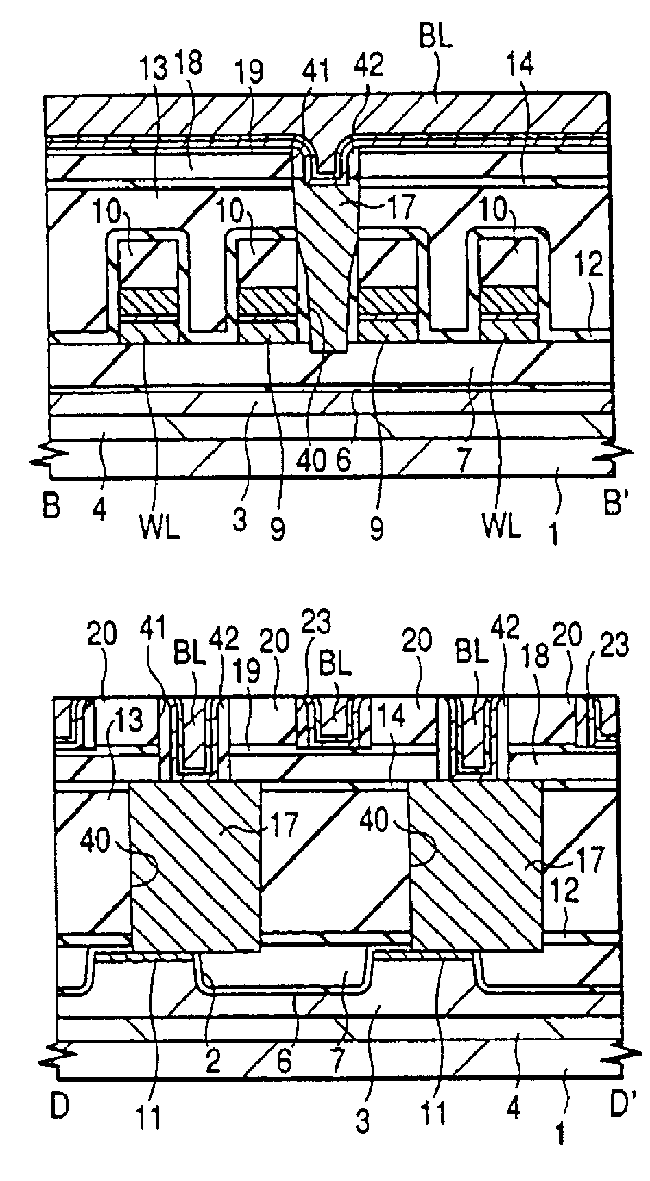
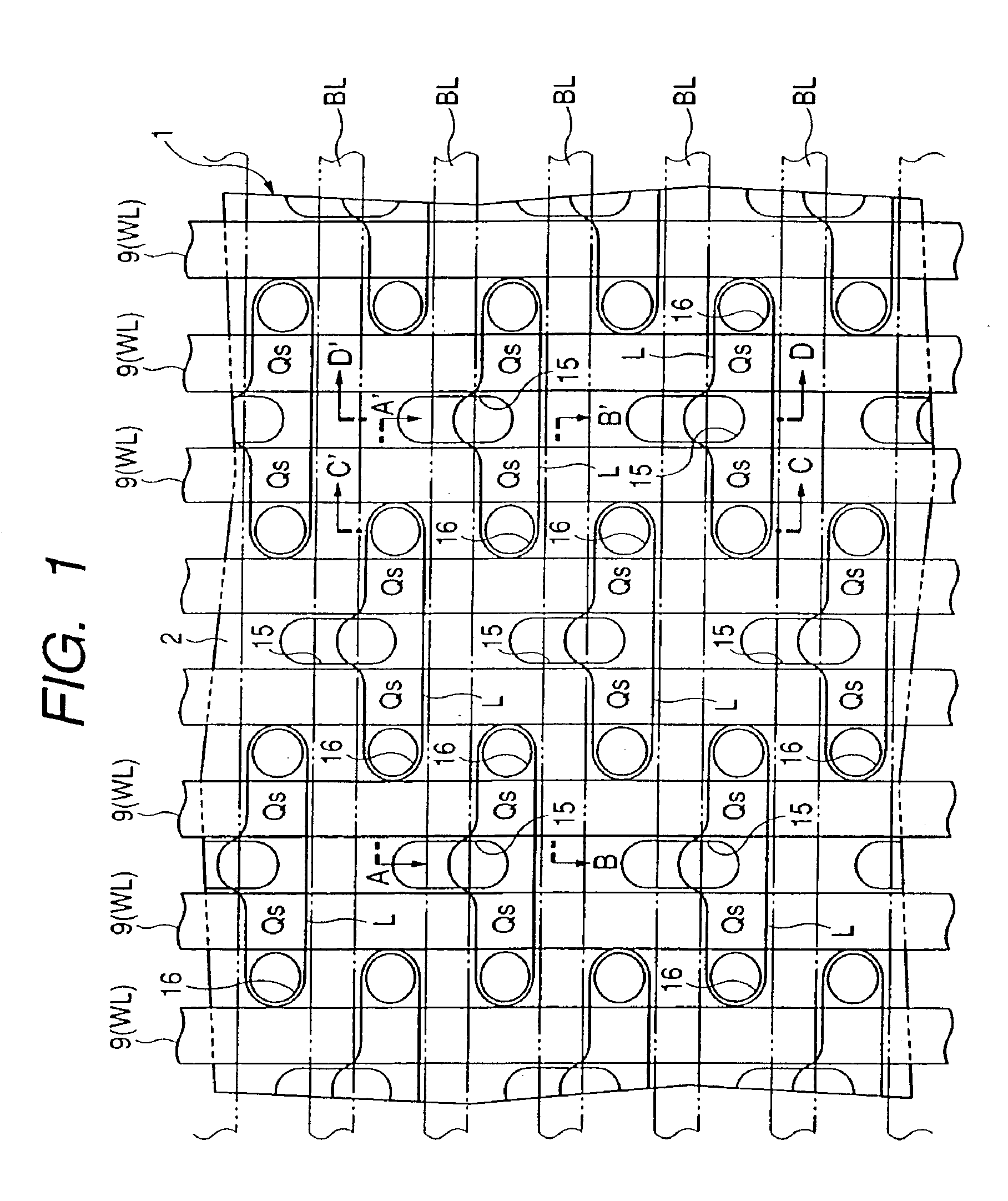
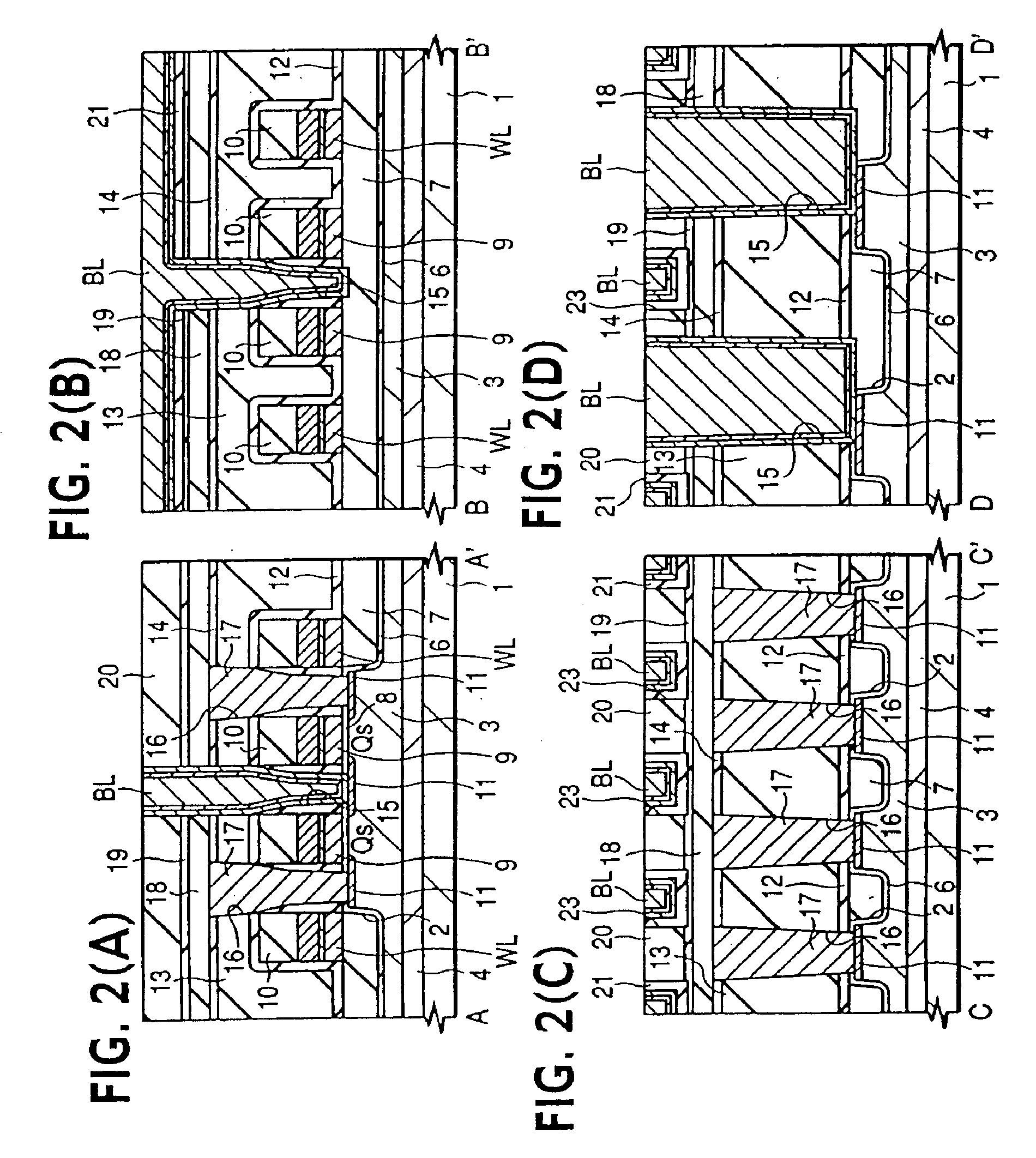
[0098]FIG. 1 is a plan view of an essential portion of a substrate showing a memory cell in the process of manufacturing a DRAM representing a preferred embodiment 1 in accordance with the present invention, and FIG. 2(A) through FIG. 2(D) are cross-sectional views of an essential portion of the substrate. In this connection, the FIG. 2(A) is a cross-sectional view taken on a line A-A′ in FIG. 1. FIG. 2(B) is a cross-sectional view taken on a line B-B′ in FIG. 1. FIG. 2(C) is a cross-sectional view taken on a line C-C′ in FIG. 1, and FIG. 2(D) is a cross-sectional view taken on a line D-D′ in FIG. 1.

[0099]On the main surface of a substrate 1 made of a p-type single crystal silicon, for example, there is formed a p-type well 3, and on the p-type well 3 there is formed active-regions L, the periphery of each of which is defined by a device isolating trench 2. As shown in FIG. 1, the active region L is formed in a plan pattern shaped as an inverted letter ...


PUM


Abstract

A memory cell of a DRAM is reduced in size by making the width of a bit line finer than the minimum size determined by the limit of resolution of a photolithography. The bit line is made fine by forming a silicon oxide film on the inside wall of a wiring trench formed in a silicon oxide film and by forming the bit line inside the silicon oxide film. The silicon oxide film formed in the trench is deposited so that the silicon oxide film has a thickness thinner than half the width of the wiring trench and in the fine gap inside the silicon oxide film is buried a metal film to be the material of the bit line.

Description

[0002]This is a divisional of parent application Ser. No. 09 / 548,966, filed Apr. 13, 2000 now U.S. Pat No. 6,762,449, the entire disclosure of which is hereby incorporated by reference.BACKGROUND OF THE INVENTION[0003]The present invention relates to a semiconductor integrated circuit device and a method of manufacturing the same; and, in particular, the invention relates to a technology applicable to a semiconductor integrated circuit device having a DRAM (dynamic random access memory).[0004]A memory cell in a DRAM is arranged at each of the points of intersection of a plurality of word lines and a plurality of bit lines, which are arranged in the form of a matrix on the main surface of a semiconductor substrate, and the memory cell is constituted by one MISFET (metal insulator semiconductor field effect transistor) for selecting the memory cell and one capacitance element (capacitor) for storing information connected in series thereto.[0005]The above-mentioned MISFET for selecting...

Claims


Application Information

Patent Timeline
Patent Type & Authority Patents(United States)
IPC IPC(8): H01L21/70H01L21/8242H01L21/768H01L21/8247H01L27/10H01L27/105H01L27/108H01L27/115H01L29/76
CPCH01L27/105H01L27/10885H01L27/11529H01L27/115H01L27/11526H01L27/10814H01L27/10855H01L27/10894H01L27/10888H10B12/315H10B12/485H10B12/09H10B12/0335H10B12/482H10B41/41H10B41/40H10B69/00H10B12/00
Inventor UCHIYAMA, HIROYUKIOGISHIMA, ATSUSHISHUKURI, SHOJI
Owner LONGITUDE LICENSING LTD
Why Eureka
Try Eureka