Method for the production of nanometer scale step height reference specimens

a technology of height reference specimens and nanometer scales, which is applied in the direction of polycrystalline material growth, after-treatment details, instruments, etc., can solve the problems of less desirable commercial step-height reference standards, height calibration artifacts not previously available, and not previously commercially availabl

Inactive Publication Date: 2005-03-22
NASA
View PDF9 Cites 45 Cited by
  • Summary
  • Abstract
  • Description
  • Claims
  • Application Information

AI Technical Summary

Benefits of technology

[0019]It is a primary object of the present invention to provide a method that yields a device particularly suited to serve as an artifact for scanning probe microscopes and profilometers and

Problems solved by technology

While the level of quantitative two or three-dimensional topographic information related to scanning probe microscopes may be critical to modern manufacturing quality control or to leading-edge research, the ideal step-height calibration artifact (herein also called a device) for measurement confidence from multiple nanometers down to the one nanometer level and below has not, from our understanding, previously been commercially available.
Typically, however, these require careful location and preservation, so generally are considered less desirable as a commercial step-height reference standard than other approaches.
One current type of step-height standard is fabricated by etching/deposition processes resulting in some undesired roughness, such as the intrinsic surface roughness of a native silicon oxide more fully described, for example, in two (2) U.S. Pat. Nos. 5,955,654; and 5,599,464, as well as in the technical brochure of Silicon MDT Ltd., POB 50,103305, made available in Moscow, Russia and represented by K-TEK International, Inc., of Portland, Oreg.
This intrinsic surfac

Method used


Image

  • Method for the production of nanometer scale step height reference specimens
  • Method for the production of nanometer scale step height reference specimens
  • Method for the production of nanometer scale step height reference specimens

Examples


Embodiment Construction

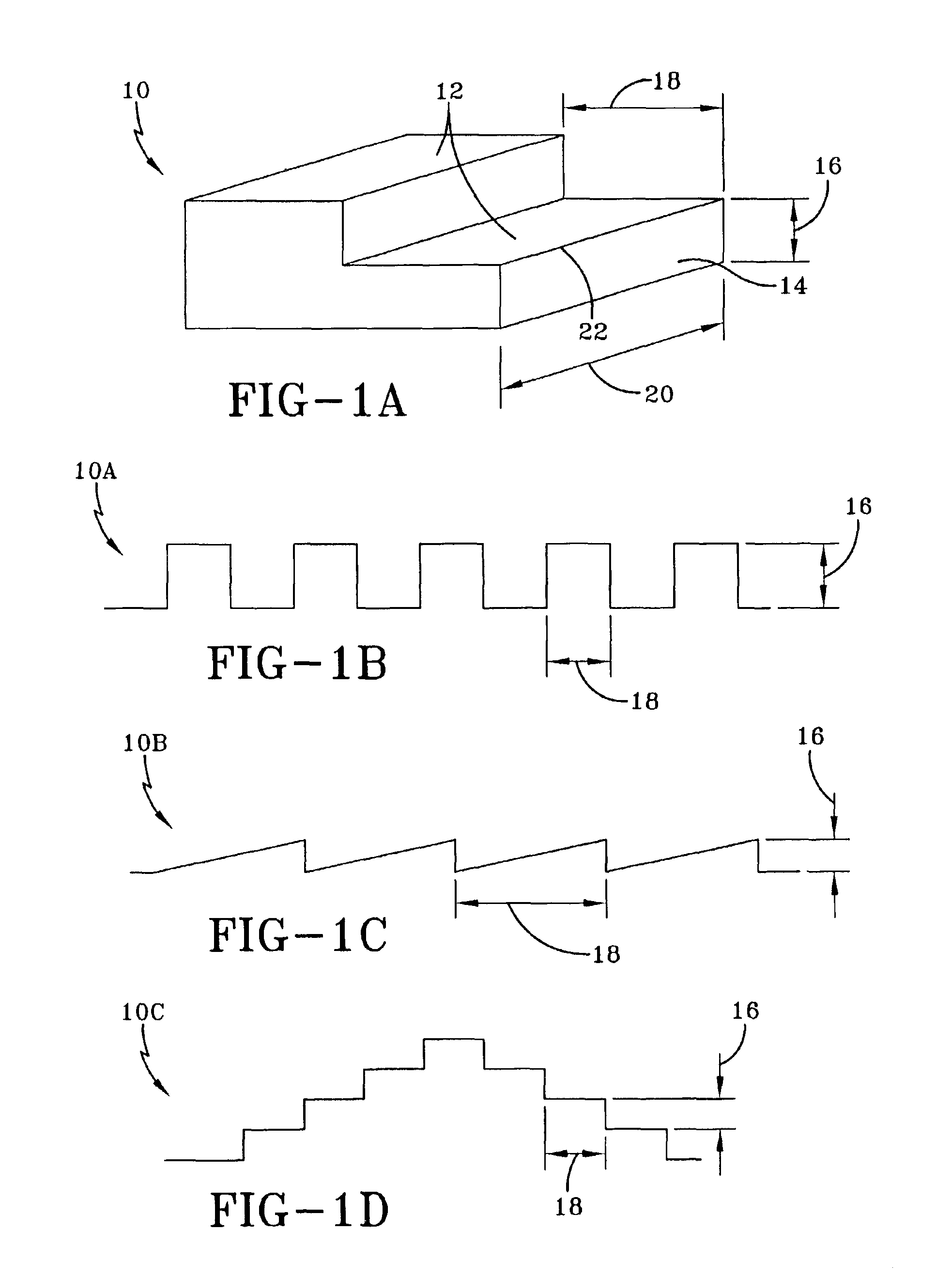
step-height from plateau to plateau.

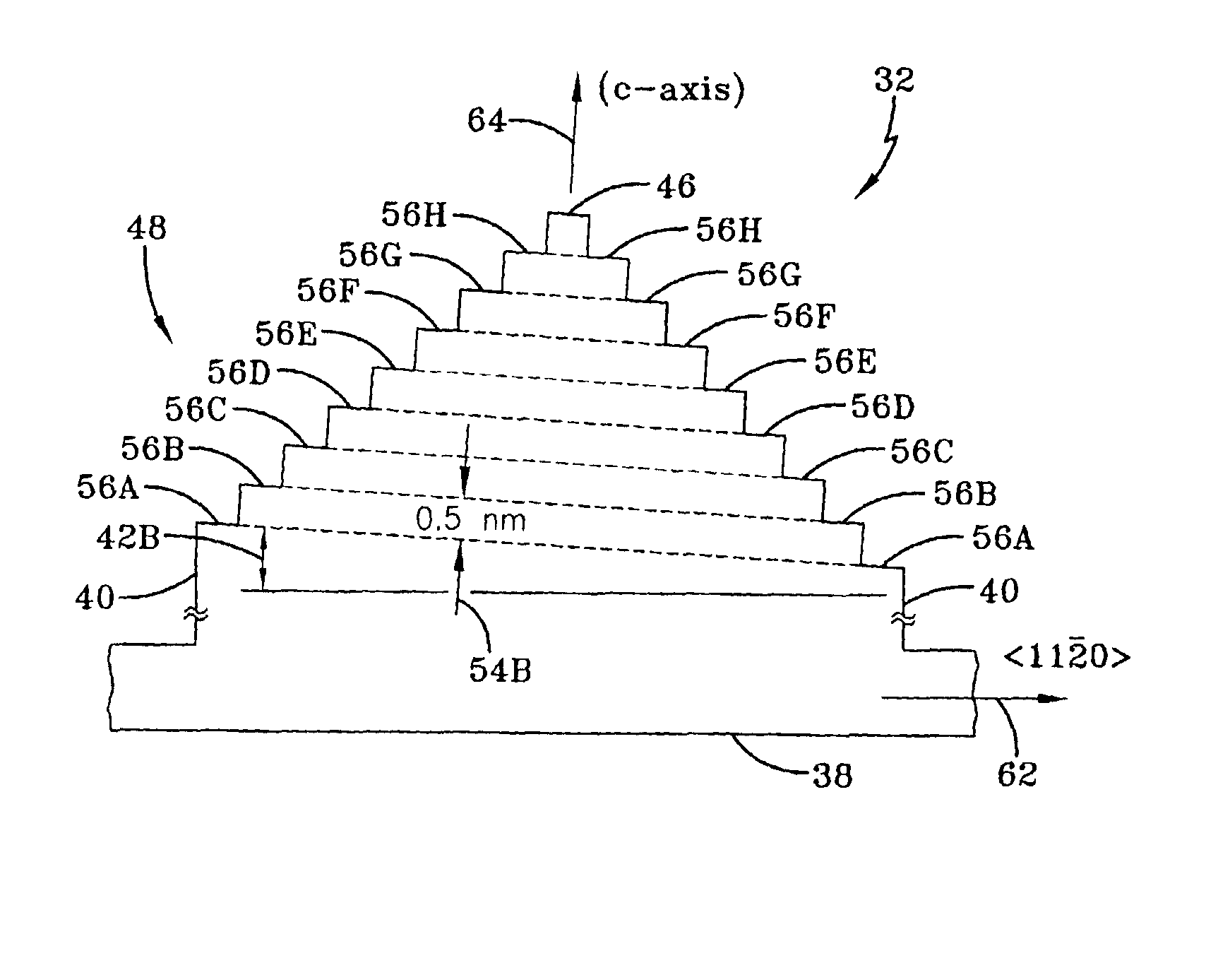
[0038]FIG. 10 is comprised of FIGS. 10A and 10B that illustrate collectively a further embodiment of the present invention, wherein the step-flow etch is carried out on a 3C-SiC single crystal heteroepitaxial film that has been grown on an atomically flat 4H-SiC mesa. The step-flow etch produces a pyramidal pattern of concentric plateaus that have a step-height of single bilayer (approximately 0.25 nm) between each plateau. The shape of the plateaus approximate the shape of the mesa. FIG. 10A is a top view of the plateaus, and FIG. 10B is a cross-sectional view showing the single-bilayer steps and the tilt of the plateaus with respect to the bottom of the wafer. For purposes of illustration, it is assumed that the initial top surface of the wafer is parallel to the bottom surface of the wafer.

DETAILED DESCRIPTION OF THE PREFERRED EMBODIMENTS

[0039]The present invention is related to a product by process, wherein the product is primarily a step-heig...


PUM


Abstract

Methods are disclosed that provide for structures and techniques for the fabrication of ordered arrangements of crystallographically determined nanometer scale steps on single crystal substrates, particularly SiC. The ordered nanometer scale step structures are produced on the top surfaces of mesas by a combination of growth and etching processes. These structures, sometimes referred to herein as artifacts, are to enable step-height calibration, particularly suitable for scanning probe microscopes and profilometers, from less than one nanometer (nm) to greater than 10 nm, with substantially no atomic scale roughness of the plateaus on either side of each step.

Description

ORIGIN OF THE INVENTION[0002]The invention described herein was made by employees of the United States Government and may be used by or for the Government for governmental purposes without payment of any royalties thereon or therefor.FIELD OF THE INVENTION[0003]The invention relates to methods, which provide for structures and techniques for the fabrication of ordered arrangements of atomic scale steps on SiC single crystal substrates. The structures consist of patterned arrays of mesas with each mesa having a pattern of steps etched and / or grown on a selected crystal plane. These structures with steps perform as physical artifacts that are particularly suited for scanning probe microscopes and profilometers to enable step-height calibration from less than one nanometer (nm) to greater than 10 nm, with no more than atomic scale roughness of the plateaus of the structures thereof on either side of each step.BACKGROUND OF THE INVENTION[0004]The current generation of commercially avail...

Claims


Application Information

Patent Timeline
IPC IPC(8): C30B33/00G12B21/20G12B21/00G01Q40/02G01Q90/00
CPCB82Y35/00G01Q40/02C30B33/00C30B29/36
Inventor ABEL, PHILLIP B.POWELL, J. ANTHONYNEUDECK, PHILIP G.
Owner NASA
Why Eureka
Try Eureka