

Compact process chamber for improved process uniformity
a process chamber and compact technology, applied in the field of process chambers, can solve the problems of adding weight to the reactor, requiring additional materials, and thick windows to resist the stresses of the chamber, so as to improve the uniformity of deposition, uniform deposition profile, and increase the thickness
- Summary
- Abstract
- Description
- Claims
- Application Information
AI Technical Summary
Benefits of technology
Problems solved by technology
Method used
Image

Examples
Embodiment Construction
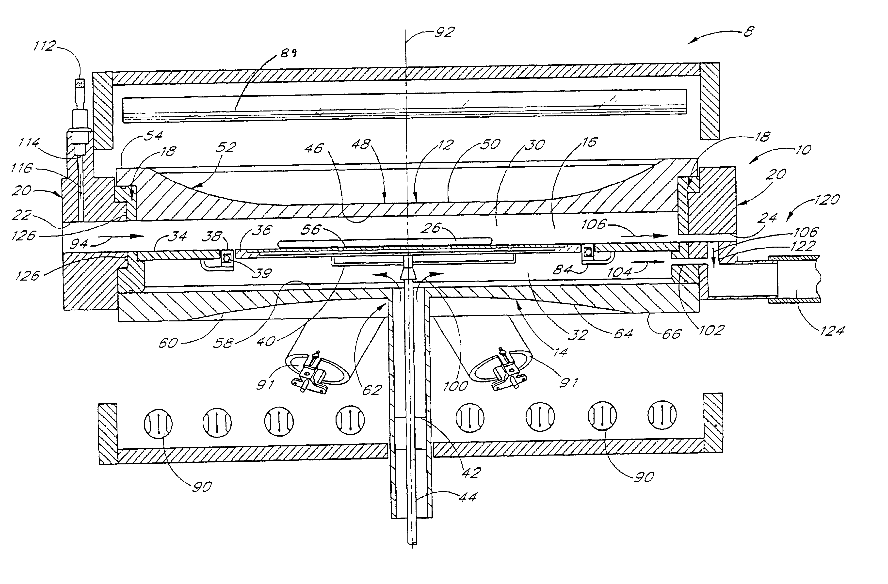
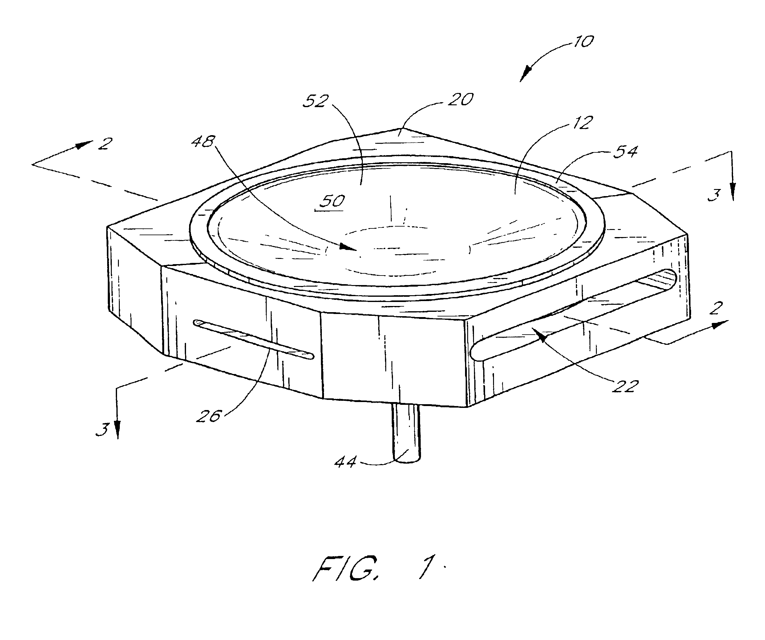
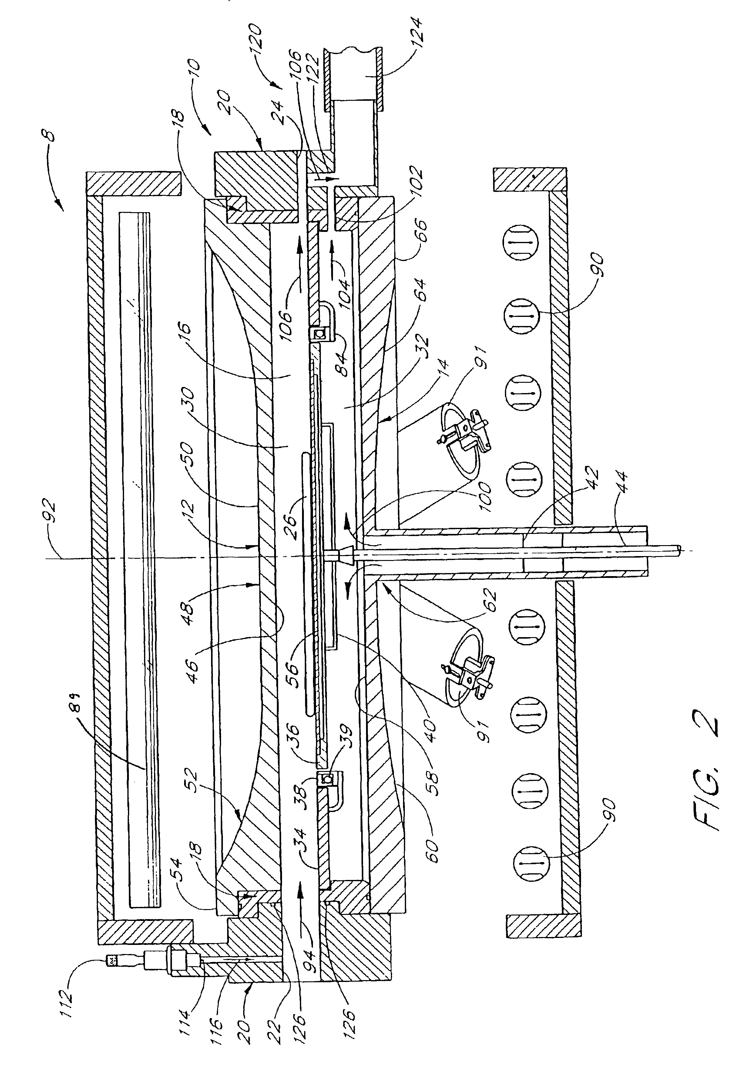
Although the chamber described herein is applicable to batch processing systems, it is of particular utility in single wafer processing systems. In particular, the chamber 10 described herein is applicable to processing of a single 300 mm silicon wafer at a reduced pressure of about 20 to 60 Torr. It should be recognized, however, that the principles of the present invention are applicable to other size wafers processed at different pressures and temperatures. The skilled artisan may also find application for the principles disclosed herein to both cold wall and hot wall reactors. Furthermore, advantages of the chamber described herein are applicable to several types of processing, including thermal annealing, deposition, etching, lithography, diffusion, and implantation.
Preferred Chamber
FIGS. 1 and 2 show a semiconductor processing reactor 8, which includes a reaction or process chamber 10, constructed in accordance with a preferred embodiment. The chamber 10 has an upper wall 12 a...
PUM
| Property | Measurement | Unit |
|---|---|---|
| width | aaaaa | aaaaa |
| width | aaaaa | aaaaa |
| width | aaaaa | aaaaa |
Abstract
Description
Claims
Application Information