
Substrate for epitaxial growth

a technology of substrates and epitaxial growth, which is applied in the direction of natural mineral layered products, instruments, transportation and packaging, etc., can solve the problems of insufficient crystallinity improvement of films, disadvantageous dispersion of al-containing group iii nitride films, and inability to achieve sufficient crystallinity improvement, etc., to achieve excellent crystallinity and further improve the crystallinity of nitride films

Active Publication Date: 2005-03-22
NGK INSULATORS LTD
View PDF9 Cites 16 Cited by
  • Summary
  • Abstract
  • Description
  • Claims
  • Application Information

AI Technical Summary

Benefits of technology

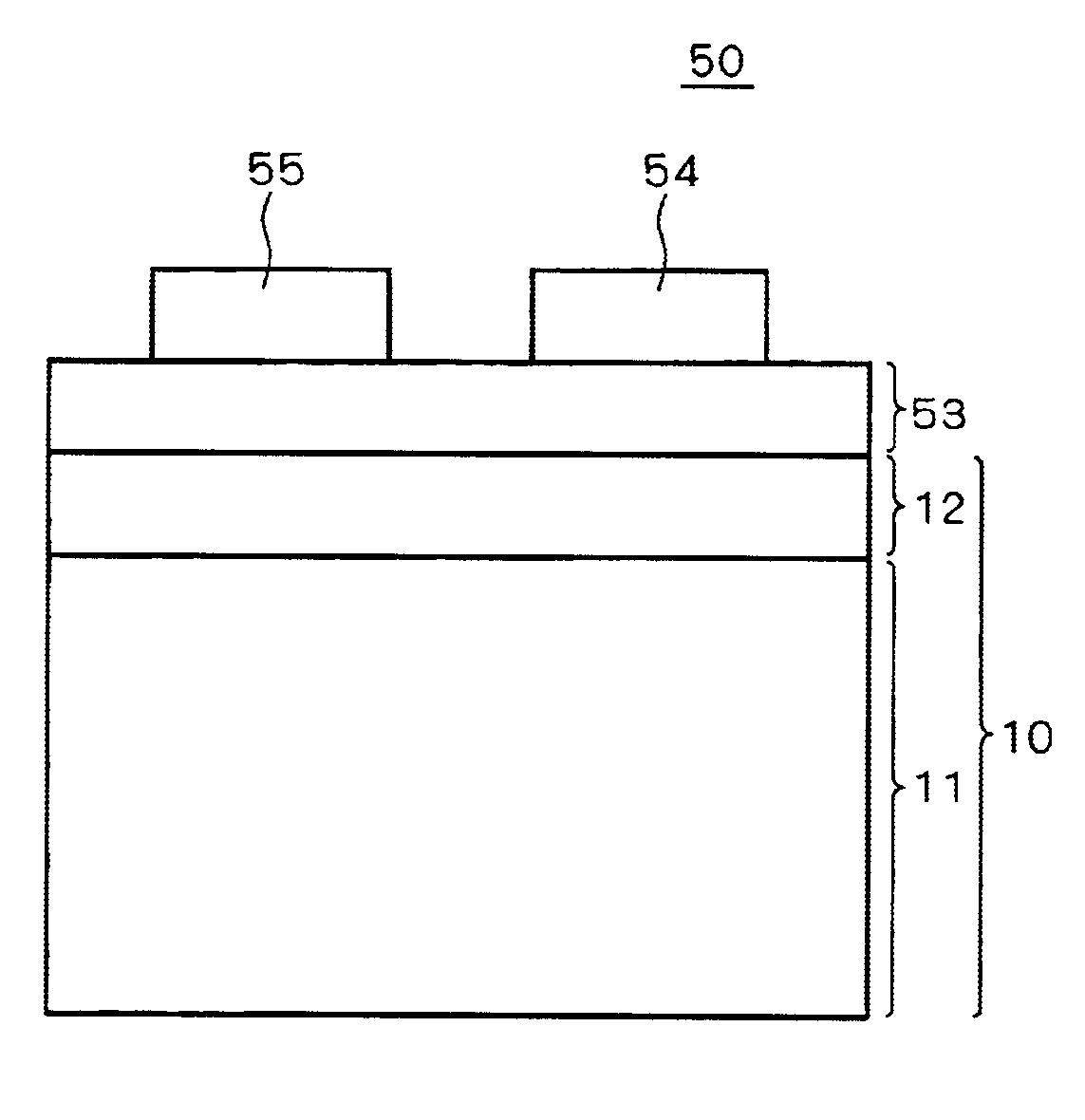
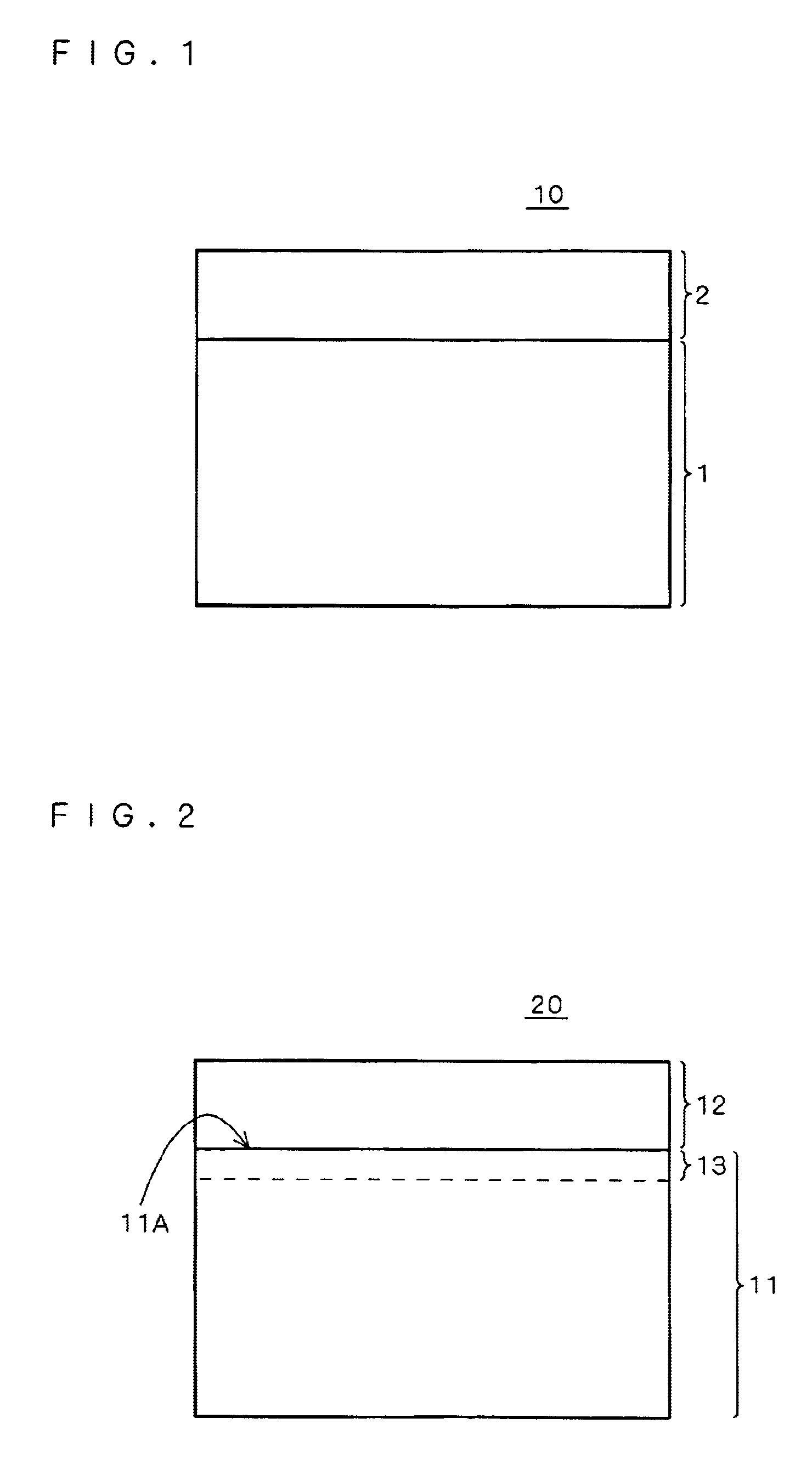
The crystal quality of one or more group III nitride films, particularly the Al-containing group III nitride films, is remarkably improved, when the one or more group III nitride films are formed on this substrate for epitaxial growth,. The characteristics of a finally obtained semiconductor device or the like are also remarkably improved.
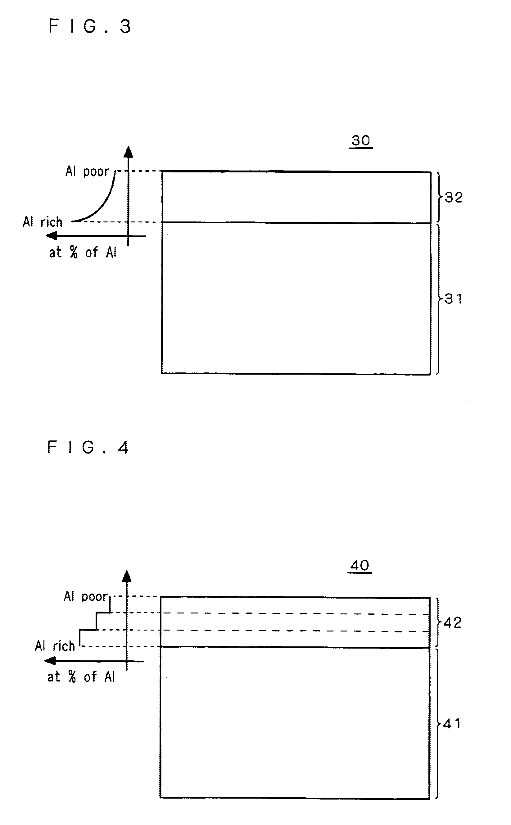
The dislocation density and crystallinity of the nitride film are further improved while no cracking is caused in the nitride film. Further, the crystal quality of one or more group III nitride films, particularly the Al-containing group III nitride films,formed on the substrate for epitaxial growth is also further improved.
Thus, the crystal quality of the nitride film is further improved, whereby the crystal quality of one or more group III nitride films, particularly the Al-containing group III nitride films, formed on the substrate for epitaxial growth is also further improved.
Accordingly, an object of the present invention is to provide a substrate for epitaxial growth allowing formation thereover of an Al-containing group III nitride film having excellent crystal quality.

Problems solved by technology

If an underlayer is formed on this buffer film for forming an Al-containing group III nitride film provided with various functions thereon, therefore, these films cannot be sufficiently improved in crystallinity.
In addition, the group III nitride film, particularly an Al-containing one, is disadvantageously remarkably dispersed in crystal quality such as crystallinity and dislocation density due to the temperature history from formation of the buffer film up to formation of the Al-containing group III nitride film.
In other words, the Al-containing group III nitride film provided with various functions cannot attain sufficiently high crystal quality in view of crystallinity and dislocation density when the sapphire base is employed for preparing the substrate for epitaxial growth.
Thus, a semiconductor light-emitting device including this Al-containing group III nitride film is deteriorated in luminous efficiency, for example.
This film is also insufficient in surface flatness due to pitting or the like.
Further, the film is disadvantageously readily influenced by defects present on the surface of the SiC base.

Method used


Image

  • Substrate for epitaxial growth
  • Substrate for epitaxial growth
  • Substrate for epitaxial growth

Examples


example 1

A 6H—SiC base having a thickness of 330 μm and a diameter of 2 inches was set in a prescribed reaction tube and heated to 1150° C. while trimethyl aluminum (TMA) and ammonia (NH3), the molar ratio of those gases are set to NH3 / TMA=0.1-500, were introduced into the reaction tube at a flow velocity of 5 m / sec., thereby forming an AlN film having a thickness of at least 0.5 μm on the 6H—SiC base. The nitrogen molar fraction on the surface of the 6H—SiC base was 2.1 atomic %.

The dislocation density of the AlN film formed with the thickness of 0.5 μm measured with a TEM (transmission electron microscope) was 2×10¹⁰ / cm2. This AlN film exhibited a full width of 80 seconds at the half maximum of the X-ray rocking curve for (002) plane and a full width of 900 seconds at the half maximum of the X-ray rocking curve for (102) plane. Further, the surface roughness of the AlN film was 1.5 Å, and a clear atomic step was clearly observed with an AFM. Under these film forming conditions, the critica...

example 2

A 6H—SiC base was set in a reaction tube and heated to 1150° C. similarly to Example 1 while NH3 was introduced along with hydrogen (H2) carrier gas for nitriding the main surface of the 6H—SiC base and forming a nitrided layer with a thickness of 1 μm. Then, an AlN film having a thickness of at least 0.5 μm was formed under the same conditions as those in Example 1. Another 6H—SiC base subjected to only nitriding under the same conditions exhibited a nitrogen molar fraction of 10.3 atomic %.

The dislocation density of the AlN film formed with the thickness of 0.5 μm measured with a TEM was 2×10¹⁰ / cm2. This AlN film exhibited a full width of 80 seconds at the half maximum of the X-ray rocking curve for (002) plane and a full width of 900 seconds at the half maximum of the X-ray rocking curve for (102) plane. Further, the surface roughness of the AlN film was 1.5 Å, and a clear atomic step was clearly observed with an AFM. Under these film forming conditions, the critical thickness ca...


PUM

PropertyMeasurementUnit
Temperatureaaaaaaaaaa
Timeaaaaaaaaaa
Timeaaaaaaaaaa

Abstract

A substrate for epitaxial growth allowing formation of an Al-containing group III nitride film having high crystal quality is provided. A nitride film containing at least Al is formed on a 6H—SiC base by CVD at a temperature of at least 1100° C., for example. The substrate for epitaxial growth allowing formation of an Al-containing group III nitride film having high crystal quality is obtained by setting the dislocation density of the nitride film to not more than 1×10¹¹ / cm2, the full width at half maximum of an X-ray rocking curve for (002) plane to not more than 200 seconds and the full width at the half maximum of the X-ray rocking curve for (102) plane to not more than 1500 seconds.

Description

This application claims the benefit of Japanese Application P2002-366679, filed Dec. 18, 2002, the entirety of which is incorporated herein by reference.BACKGROUND OF THE INVENTION1. Field of the InventionThe present invention relates to a substrate for epitaxial growth employed as the substrate for various types of semiconductor devices.2. Description of the Background ArtAn Al-containing group III nitride film is employed as a semiconductor film constituting a semiconductor light-emitting device or a semiconductor photoreceptor or an underlayer for growing this semiconductor film. In recent years, the Al-including group III nitride film has also been remarked as a semiconductor film constituting an electronic device such as a high-speed IC chip employed for a portable telephone or the like or a shortwave LED.The aforementioned semiconductor device is obtained by forming a buffer layer consisting of a group III nitride on a single-crystalline base consisting of a single crystal of ...

Claims


Application Information

Patent Timeline
IPC IPC(8): C30B25/18C30B25/02H01L21/20H01L21/02C30B29/38H01L21/205
CPCC30B25/02C30B25/18C30B29/403H01L21/02378H01L21/02458H01L21/0254H01L21/0262H01L21/0243Y10T428/12528Y10T428/265
Inventor SHIBATA, TOMOHIKOSUMIYA, SHIGEAKIASAI, KEIICHIROTANAKA, MITSUHIRO
Owner NGK INSULATORS LTD
Learn More