Input/output circuit with user programmable functions

a user-programmable, input/output circuit technology, applied in the field of integrated circuits, can solve the problems of large setup time relative to the same clock signal, large switching noise, and unpredictable signals at the output of the register, and achieve the effect of optimal flexibility and performan

Inactive Publication Date: 2005-03-22
XILINX INC
View PDF13 Cites 57 Cited by
  • Summary
  • Abstract
  • Description
  • Claims
  • Application Information

AI Technical Summary

Benefits of technology

The I / O circuit of the present invention provides optimal flexibility and performance using a number of different structures and methods.

Problems solved by technology

The amount of switching noise produced is in part attributable to the amount of overshoot occurring in the transition of the clock signal from one logic state to another.
If a data signal changes during the setup time or hold time, the signal at the output of the register is unpredictable.
However, as the hold time relative to a clock signal becomes more negative, the setup time relative to the same clock signal becomes larger.
Unfortunately, more flexible programmability of the CSL causes more complex CSL production testing procedures.
The cost of production of the CSL increases with the increase in complexity of CSL testing procedures.
During programming of the configuration memory elements, the internal logic of the CSL is unstable and unpredictable.
A conventional pull-up circuit as described above limits the flexibility of a system designer by limiting the options available for defining a given logic state on the output pad.
However, the number of channels available for a direct connection to a input terminal providing input signals is seriously limited.
However, this latching or registering significantly increases the circuit area as well as the delay involved in selecting signals for routing.
Although the function and connectivity of the tile at each edge may be individually customized to take particular advantage of the location of the tile, the expense of this customization is greatly increased effort for design, verification, and layout.

Method used


Image

  • Input/output circuit with user programmable functions
  • Input/output circuit with user programmable functions
  • Input/output circuit with user programmable functions

Examples


Embodiment Construction

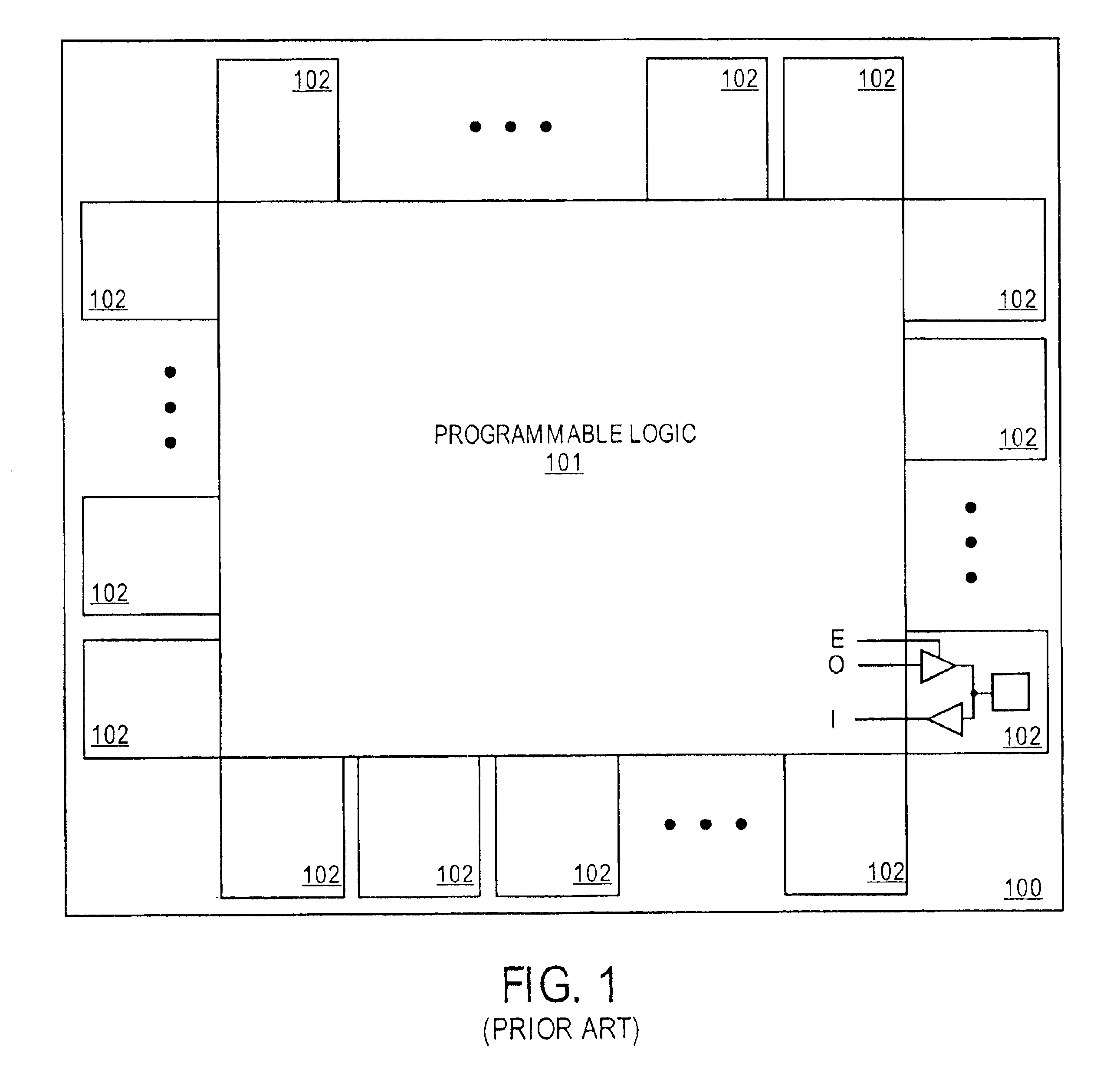
FIG. 1 is a block diagram of a conventional field programmable logic device (FPLD) 101 including IOBs 102. IOBs 102 provide an interface with external circuitry.

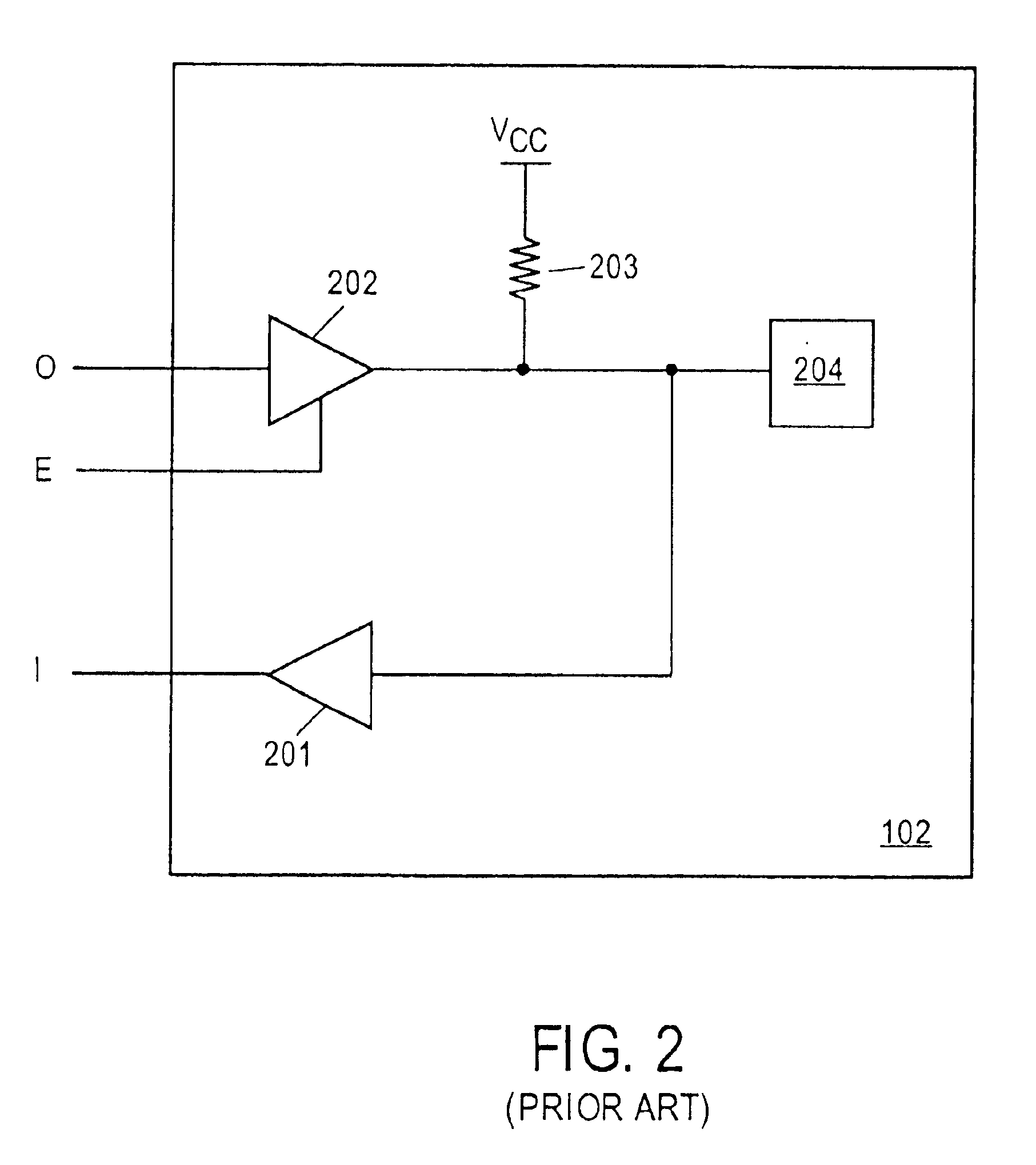
FIG. 2 is a schematic diagram of a conventional circuit to implement one of IOBs 102 of FPLD 101. IOB 102 includes buffers 201-202, pull-up resistor 203, and I / O pad 204. This conventional pull-up circuit limits the flexibility of a system designer by limiting the options available for defining a given logic state on the output pad.

FIG. 3 is a schematic diagram of a Configurable System on a Chip (CSoC) in accordance with an embodiment of the present invention.

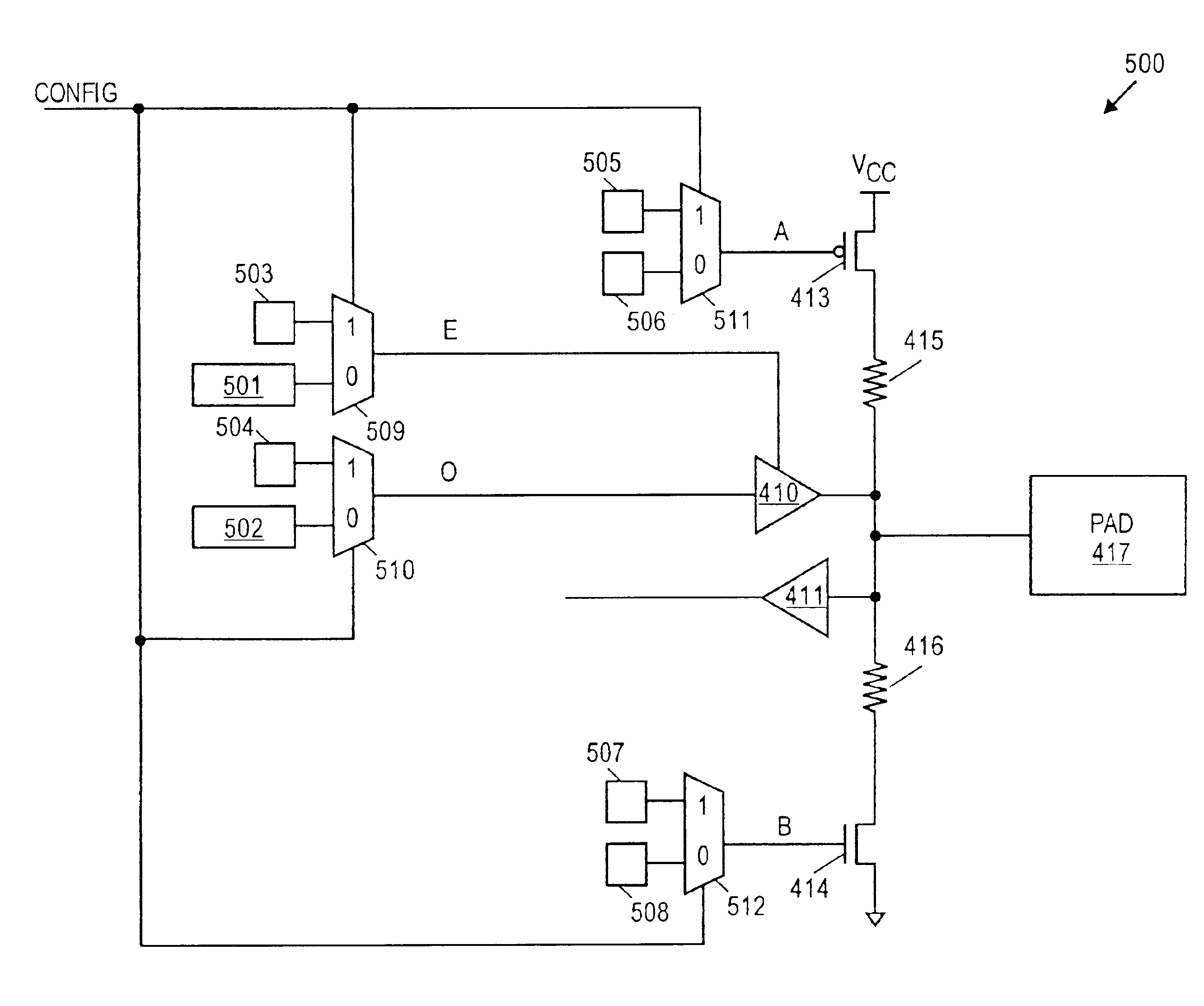
FIG. 4 is a schematic diagram of CSL PIO 400 in accordance with an embodiment of the present invention. The I signal is the input data signal to the CSL from I / O pad 417. The signal is the output data signal from the CSL to I / O pad 417. The E signal is the output enable signal for PIO 400. The cf_pu signal is the configuration pull-up signal and the cf_pd signal is the ...


PUM


Abstract

The I/O circuit of the present invention provides optimal flexibility and performance using a number of different structures and methods. The present invention provides a signal follower circuit for an input pad. In one embodiment, the output buffer is capable of injecting a constant onto a pad during reconfiguration of a configurable system logic circuit. The present invention also provides a circuit for generating a programmable data propagation delay, thereby guaranteeing zero hold time for an arbitrary input register. Zero hold time is accomplished by allowing the user to optimally characterize clock delay to a given input/output circuit. The present invention also provides fast switching between input pads, thereby minimizing data propagation delay between the input pads. Additionally, the present invention reduces time spent in production product test by facilitating the testing of multiple routes with one test configuration. A circuit expanding the number of data input channels available to system routing is provided. Lastly, a plurality of identical input/output block tiles (IOBTs) is disclosed, thereby enabling each I/O circuit to provide the same signals regardless of the IOBTs location in the I/O circuit.

Description

FIELD OF THE INVENTIONThe present invention relates to integrated circuits, such as configurable system logic devices and configurable system-on-chip products. More specifically, the present invention relates to a method and structure to provide an input / output circuit with user programmable functions.DISCUSSION OF RELATED ARTThe input / output (I / O) circuit of a conventional integrated circuit (IC) acts as an interface between the integrated circuit and the outside world. Conventional ICs have pre-determined internal wired connections. In general, the signals passed through the I / O circuit of a conventional non-programmable IC are pre-defined and come from hardwired locations. As a result, the I / O pins of the IC have known state requirements. For example, a particular I / O pin may need to be grounded when it is not receiving a signal from an external source.Typical circuitry within a conventional I / O circuit includes buffers (input and output) and registers (for input, output, and out...

Claims


Application Information

Patent Timeline
Patent Type & Authority Patents(United States)
IPC IPC(8): H03K19/177
CPCH03K19/17744
Inventor FOX, BRIANPAPALIOLIOS, ANDREASWINEGARDEN, STEVEN P.CHEUNG, EDMOND Y.
Owner XILINX INC
Why Eureka
Try Eureka