Magnetic head, and the magnetic read-write devices, and the magnetic memory with magnetic sensors

a magnetic read-write device and magnetic sensor technology, applied in the field of magnetic head, can solve the problems of difficult resistance measurement and element cannot be applied to an actual writing head, and achieve the effects of high magnetic resistance change coefficient, large gmr output, and high sensitivity

Inactive Publication Date: 2005-04-05
HITACHI LTD
View PDF9 Cites 22 Cited by
  • Summary
  • Abstract
  • Description
  • Claims
  • Application Information

AI Technical Summary

Benefits of technology

Since the magnetoresistive element constituted as described above has the pinned layer containing the half-metal, the second magnetic layer or the half-metallic layer, it has high magnetic resistance change coefficient or the electric resistance. Accordingly, a magnetic head of high sensitivity and large GMR output can be attained by mounting the magnetoresistive element. Further, the magnetic resistive element can also be mounted to a memory cell of a magnetic memory and can provide a magnetic memory in which the cell area can be decreased and the memory capacitance can be increased twice or more compared with usual memories.

Problems solved by technology

However, since the magnetic resistance change coefficient in the existent CPP-GMR element is too small, it involves a problem that the element can not be applied to an actual writing head.
Further, since the resistance value is too small when the element area is decreased, it results in a problem of making measurement of the resistance R difficult.

Method used


Image

  • Magnetic head, and the magnetic read-write devices, and the magnetic memory with magnetic sensors
  • Magnetic head, and the magnetic read-write devices, and the magnetic memory with magnetic sensors
  • Magnetic head, and the magnetic read-write devices, and the magnetic memory with magnetic sensors

Examples


experiment 1

[Experiment 1]

At first, a half-metal containing layer was formed on a substrate and then a noble-metallic layer was formed between the substrate and the half-metal containing layer and the following study was made for them.

Films were formed on substrates such as glass substrate, magnesium oxide substrate, GaAs substrate, AlTiC substrate, SiC substrate, Al2O3 substrate, and SiO2 substrate. An RF sputtering was used for the film preparation method. The vacuum degree attained was 5×10⁻³ Pa or lower and a target was a sintered target of Fe3O4. Films were grown in an Ar atmosphere at a pressure of 1 to 0.1 Pa and with a power of 50 W to 150 W. The film growing rate was less than 0.1 A / s. Alternatively, formation of Fe3O4 was confirmed in a case of forming the films at an extremely slow film forming rate of about 0.1 to 0.01 A / S also by using Fe as an evaporation source by a molecular beam epitaxially (MBE) method and using a method of introducing oxygen into the atmosphere while vapor de...

example 1

Then, the magnetoresistive element according to this invention is to be described.

At first, a stacked film comprising CoFe (3 nm) / GMR spacer (X nm) / Fe3O4 (50 nm) / noble-metallic film (10 nm) was prepared in order to examine the property of a spin valve element using a spacer containing a noble metal in a GMR structure film having a magnetic oxide film (pinned layer) containing an magnetic oxide material (half-metal) and a free layer containing a metal magnetic material. When the dependence of the resistance change coefficient on the thickness of the GMR spacer upon flowing a current along a film plane was examined, it showed a resistance change coefficient of about 0.3 to 1.0% at a room temperature. The value is small because this is a magnetic resistance within a plane for a film having a large resistance of half-metal portion, and the oscillation phenomenon for the resistance change coefficient depending on the thickness of the GMR intermediate layer inherent to GMR was confirmed.

T...

example 2

The film shown in FIG. 6 or FIG. 7 is applied as a magnetoresistive element of a CPP-GMR structure. The basic properties required for the CPP-GMR film includes the following three points.(a) Surface resistance of film of 2 Ωμm2 or less, preferably, 1 Ωμm2 or less (while varying depending on the element area)(b) Magnetic resistance change coefficient of 2% or higher(c) Coercive force of magnetic material

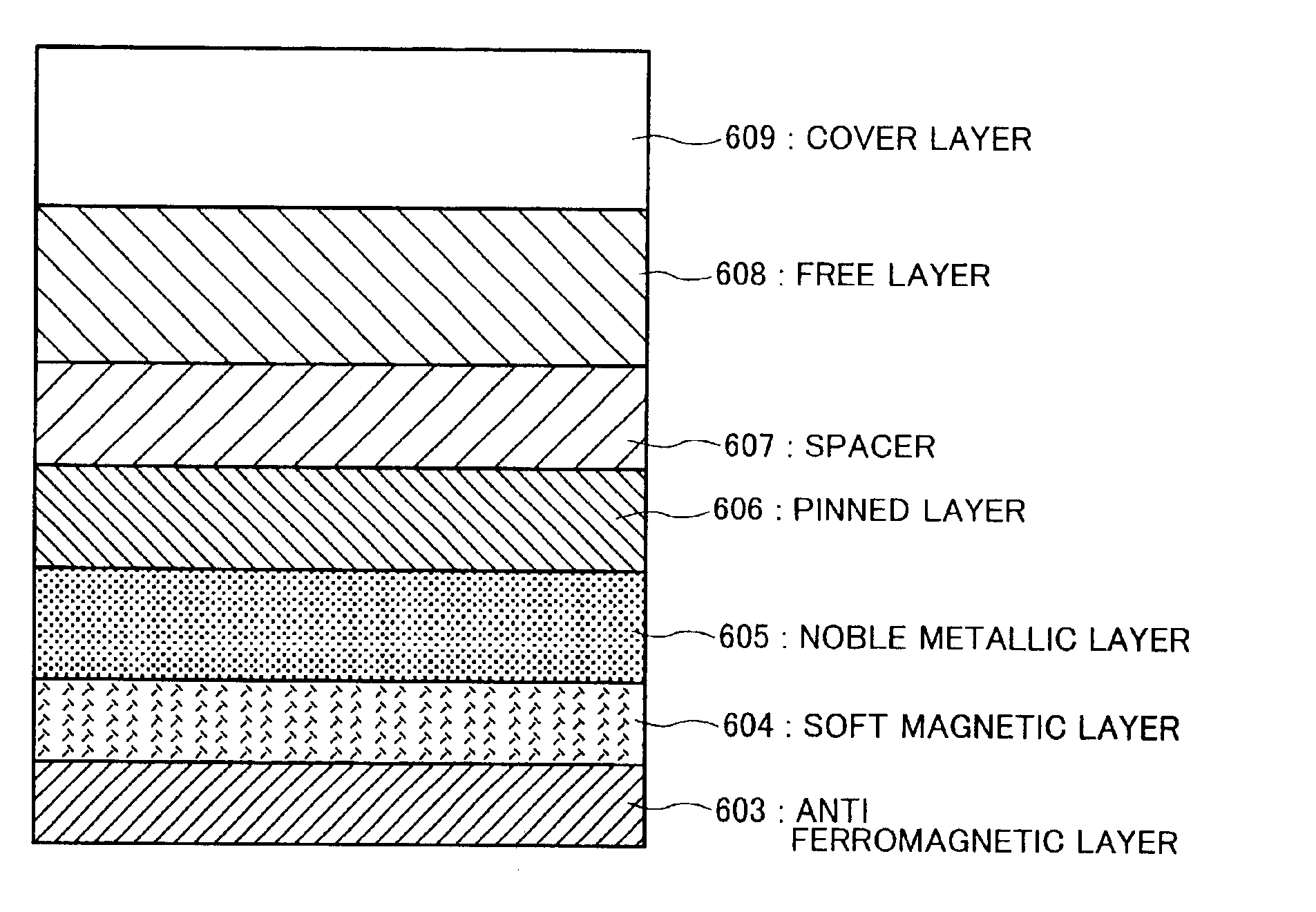
For the area resistance (a), it will be anticipated a problem different from a material of low resistance in a case of using a magnetic oxide such as Fe3O4 for the half-metal in the element. Assuming a basic structure of noble-metallic layer 605, 706 / half-metal oxide-containing pinned layer 605, 705 / noble metal-containing spacer 607, 704 / magnetic material-containing free layer 608, 703, the change of the area resistance when the thickness of Fe3O4 layer is changed for Pt (10 nm thickness) / Fe3O4 / Au (3 nm thickness) / NiFe (5 nm thickness) is calculated for an element sized 120 nm×120 nm....


PUM

PropertyMeasurementUnit
thicknessaaaaaaaaaa
areaaaaaaaaaaa
resistanceaaaaaaaaaa

Abstract

A magnetic head at high sensitivity and with enhanced output having a magnetoresistive element of high output and optimal for use in CPP-GMR, the magnetoresistive element comprising a pinned layer 606 containing a half-metal, a free layer 608 formed on one main surface of the pinned layer 606, a spacer 607 formed between the pinned layer 606 and the free layer 608, an anti-ferromagnetic layer 603 formed on the main surface of the pinned layer 606, a soft magnetic layer 604 formed between the pinned layer 606 and the anti-ferromagnetic layer 606, and a noble-metallic layer 605 formed between the pinned layer 606 and the soft magnetic layer.

Description

BACKGROUND OF THE INVENTION1. Field of the InventionThe present invention relates to a magnetic head having a magnetoresistive element and a magnetic read-write device, as well as a magnetic memory.2. Description of Related ArtIn magnetic read-write devices, recording density has been improved remarkably. Magnetic read-write heads equipped in the magnetic read-write devices are required to have high performance for both of reading and writing characteristics.Performance of the reading head can be enhanced by an anisotropic magnetoresistive (AMR) head for the recording density of 1 to 10 (Gb / in2) and by a giant magnetoresistive (GMR) head capable of attaining higher sensitivity for the recording density of 10 to 30 (Gb / in2). In the recording density of 20 to 70 (Gb / in2)at present, higher recording density of the writing head has been coped with by the advanced GMR effect referred to as specula GMR or NOL-GMR.However, along with progress for further higher sensitivity, a writing syste...

Claims


Application Information

Patent Timeline
Patent Type & Authority Patents(United States)
IPC IPC(8): G11B5/39G11B5/31G11C11/14G11C11/15H01F10/16H01F10/30H01F10/32H01L21/8246H01L27/105H01L43/08
CPCB82Y10/00B82Y25/00G11B5/3909G11B5/3903G11B5/3163G11B2005/3996G11B5/3932
Inventor TAKAHASHI, HIROMASASOEYA, SUSUMUHAYAKAWA, JUNITO, KENCHI
Owner HITACHI LTD
Why Eureka
Try Eureka