Resist material and exposure method

a technology of resist material and exposure method, which is applied in the direction of photosensitive materials, instruments, photomechanical equipment, etc., can solve the problems of deterioration of resist pattern, inability to use resins as resist materials for vuv lithography, and inability to exhibit satisfactory etching resistance of layers, etc., to achieve efficient reduction of the optical absorption rate of an alicyclic group in the wavelength range of vuv light, and the effect of increasing the rate of hydrogen atoms

Inactive Publication Date: 2005-04-19
SONY CORP
View PDF1 Cites 4 Cited by
  • Summary
  • Abstract
  • Description
  • Claims
  • Application Information

AI Technical Summary

Benefits of technology

[0020]Further, an organic material has a feature such that, the larger the rate of the hydrogen atoms in the organic material substituted by fluorine atoms, the poorer the etching resistance of the organic material. Therefore, also from the viewpoint of this, it is desired that the rate of the hydrogen atoms in the aromatic ring or alicyclic group substituted by fluorine atoms is as small as possible.
[0021]According to the present invention, the optical absorption of an alicyclic group in the wavelength range of a VUV light can be efficiently lowered with respect to the resist material or resist layer, so that favorable resist pattern can be obtained, thus enabling a more improved ultra-fine processing than before, for example, realizing processing of an ultra-fine pattern as small as 0.1 μm or less.

Problems solved by technology

However, a general organic material conventionally used as a resist material in lithography has a problem in that it exhibits high optical absorption in the wavelength range of a VUV light, and thus the light radiated does not reach the bottom portion of the resist layer, so that a preferable rectangular resist pattern cannot be formed, causing deterioration of the resist pattern.
Therefore, these resins cannot be used as a resist material for VUV lithography.
However this method poses problems in that the resist layer cannot exhibit a satisfactory etching resistance due to the small thickness of the resist, and that the small thickness of the resist causes the number of defects in the resist layer to increase.
However, the surface-imaging method has problems in that the resist pattern suffers an edge roughness, and that the dimensional control property is unsatisfactory.

Method used


Image

  • Resist material and exposure method

Examples


embodiment

[0039]Herein below, the present invention will be described with reference to the following embodiment based on experimental results.

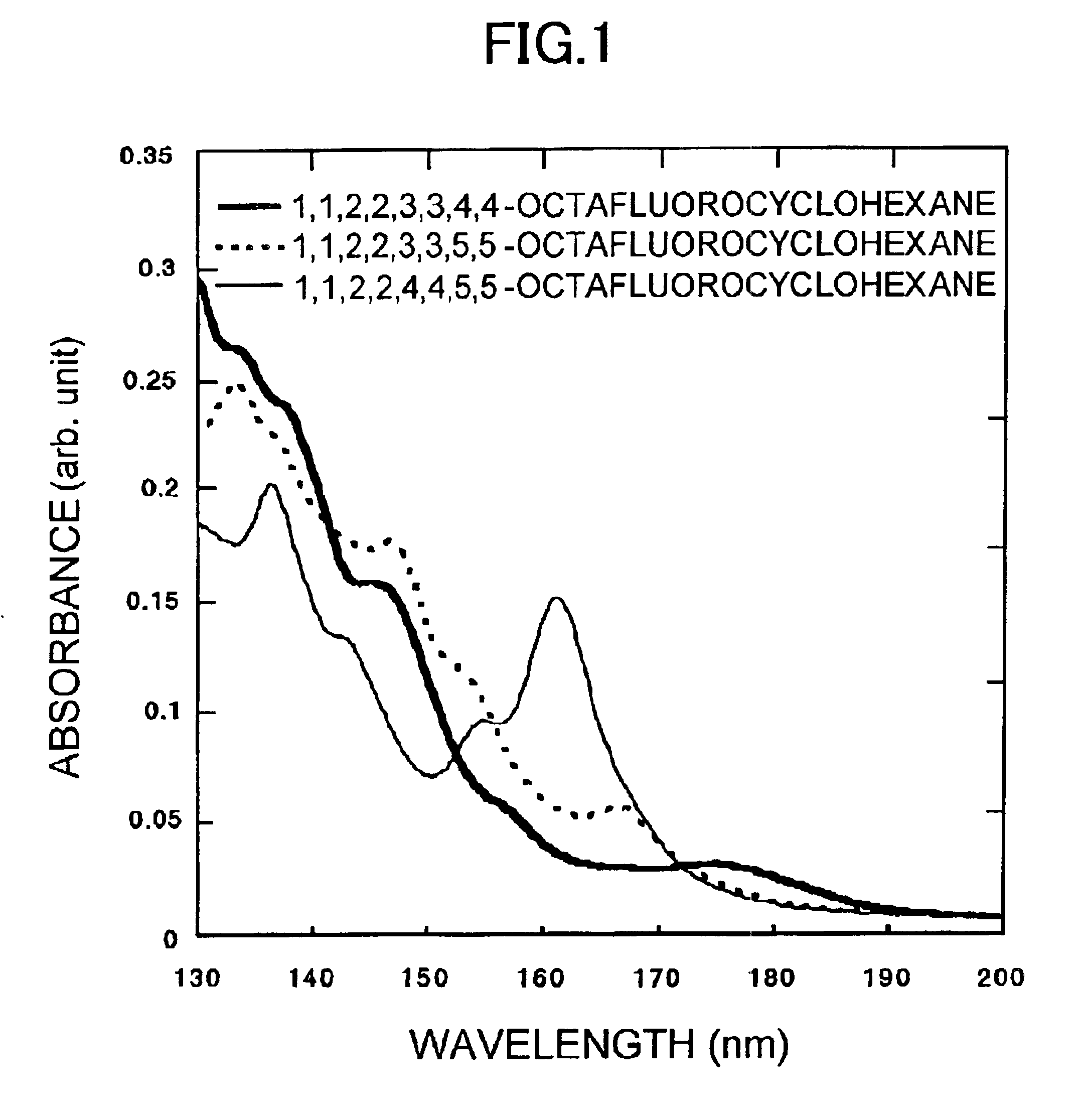
[0040]With respect to 1,1,2,2,3,3,4,4-octafluorocyclohexane, 1,1,2,2,3,3,5,5-octafluorocyclohexane, and 1,1,2,2,4,4,5,5-octafluorocyclohexane, absorption spectra in the wavelength range of a VUV light were actually measured. In the measurement of absorption spectra, a measurement apparatus was fabricated by the inventor of the present invention, and the light source used was a deuterium lamp (30 W) and an MgF2 lens was used as a light source optical system. As a spectroscope part, a concave-surface diffraction grating having 1,200 grooves / mm (with MgF2 coating) was used. The reciprocal linear dispersion was about 4 nm, and the range of the wavelength for measurement was 125 to 300 nm. In the sample chamber kept under vacuum, a semi-double beam measurement was possible, and a window gas cell made of MgF2 was disposed. A sample molecule gas having contro...


PUM

PropertyMeasurementUnit
absorption coefficientaaaaaaaaaa
wavelengthaaaaaaaaaa

Abstract

An exposure method comprising a step of subjecting a resist layer to selective exposure to an ultraviolet light and forming a predetermined pattern in the resist layer, wherein a polymer material having introduced thereinto a cyclohexane group is used as a polymer material constituting the resist layer wherein all hydrogen atoms bonded to four continuously adjacent carbon atoms in the cyclohexane group are substituted by fluorine atoms. The use of a polymer material having a lowered absorption in the wavelength range of a vacuum ultraviolet (VUV) light in the resist material or resist layer enables a more improved ultra-fine processing than before.

Description

CROSS REFERENCE TO RELATED APPLICATIONS[0001]The present document is based on Japanese Priority Document JP2001-386306, filed in the Japanese Patent Office on Dec. 19, 2001, the entire contents of which being incorporated herein by reference.BACKGROUND OF THE INVENTION[0002]1. Field of the Invention[0003]The present invention relates to a resist material and an exposure method which are used in microfabrication in, for example, the field of semiconductor.[0004]2. Description of Related Art[0005]In, for example, the field of semiconductor, as the degree of integration of semiconductor devices is increasing, an urgent task is to establish a new processing technique which enables processing of an ultra-fine pattern as small as, for example, 0.1 μm or less.[0006]A so-called lithography technique is indispensable to processing of a fine pattern. For improving the optical resolution in the lithography technique by using a light for exposure having a shorter wavelength to apply the lithogr...

Claims


Application Information

Patent Timeline
Patent Type & Authority Patents(United States)
IPC IPC(8): G03F7/038G03F7/039G03F7/004G03F7/032C08L101/04H01L21/027
CPCG03F7/0046G03F7/0382G03F7/0392Y10S430/108Y10S430/106
Inventor MATSUZAWA, NOBUYUKI
Owner SONY CORP
Why Eureka
Try Eureka