

Method of fabricating CMOS inverter and integrated circuits utilizing strained surface channel MOSFETS
- Summary
- Abstract
- Description
- Claims
- Application Information
AI Technical Summary
Benefits of technology
Problems solved by technology
Method used
Image

Examples
Embodiment Construction
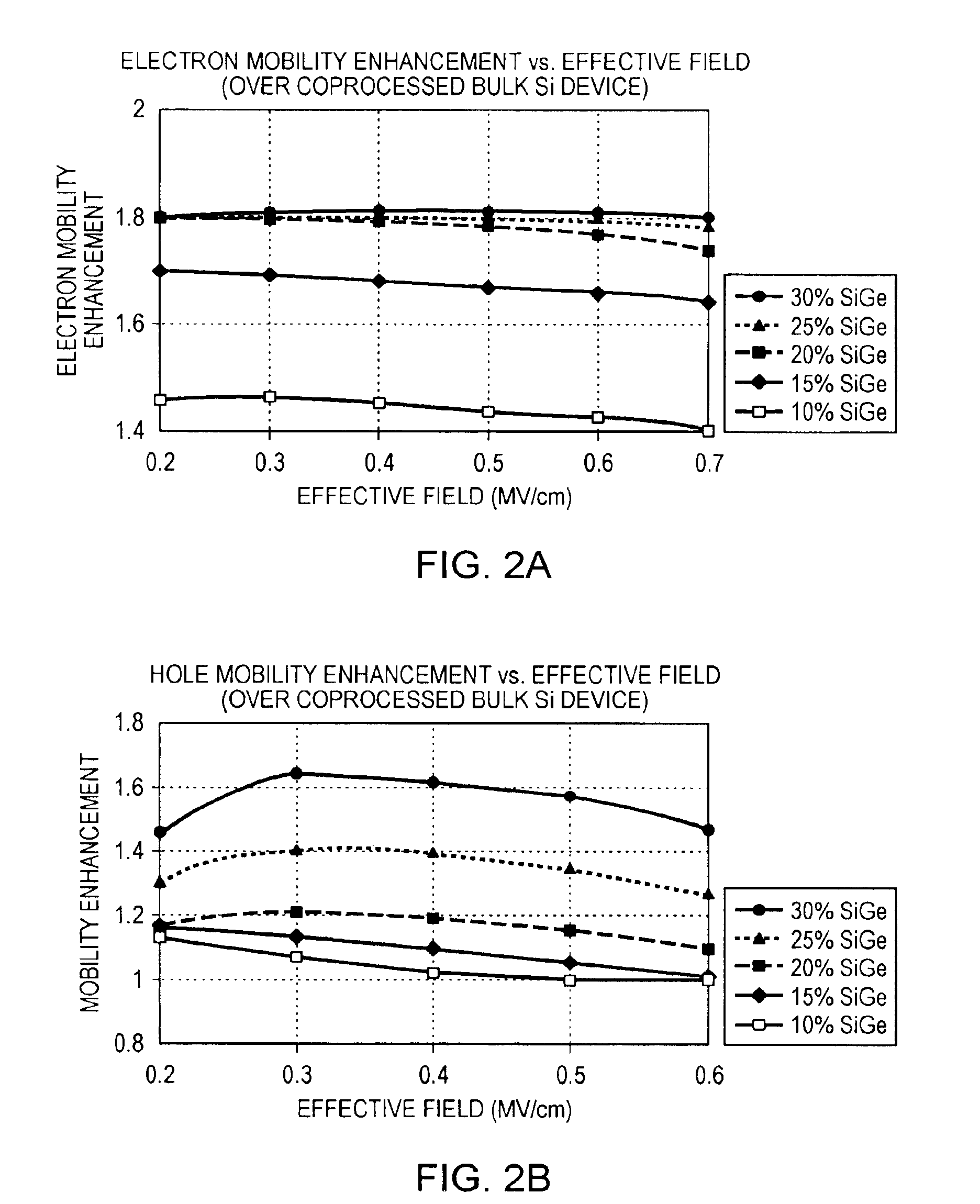
Strained Silicon Enhancement
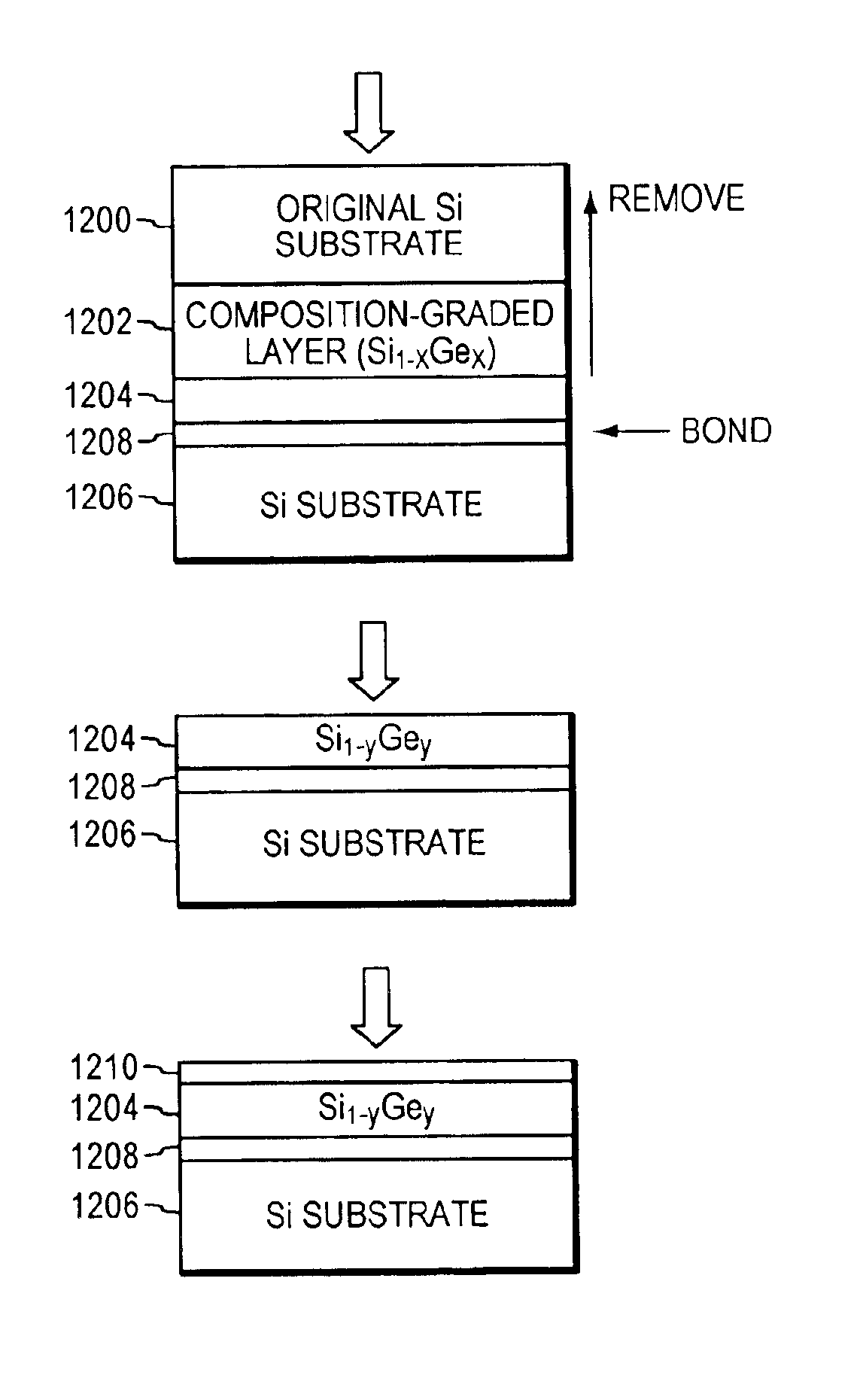
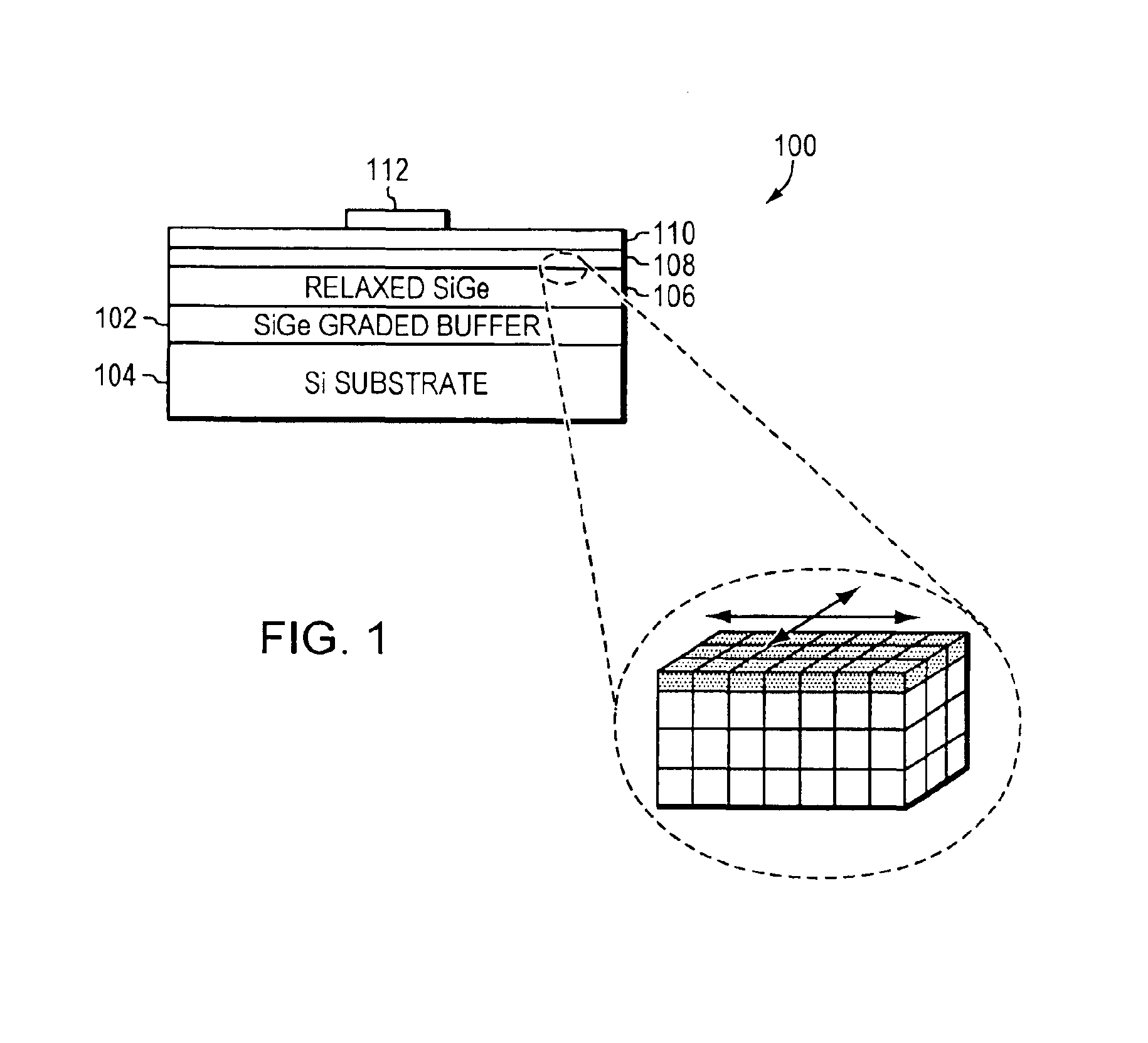
[0025]FIG. 1 is a cross-section of the substrate structure 100 required to produce a strained silicon surface channel MOSFET. The larger lattice constant, relaxed SiGe layer applies biaxial strain to the silicon surface layer. In this structure, a compositionally graded buffer layer 102 is used to accommodate the lattice mismatch between a relaxed SiGe film 106 and a Si substrate 104. By spreading the lattice mismatch over a distance, the graded buffer minimizes the number of dislocations reaching the surface and thus provides a method for growing high-quality relaxed SiGe films on Si. Subsequently, a silicon film 108 below the critical thickness can be grown on the SiGe film. Since the lattice constant of SiGe is larger than that of Si, the Si film is under biaxial tension and thus the carriers exhibit strain-enhanced mobilities. Thereafter, a layer 110 of SiO2 and a gate 112 are provided thereon.
[0026]In the structure shown in FIG. 1, the silicon channe...
PUM
 Abstract
Description
Claims
Application Information