Methods for continuous embedded process monitoring and optical inspection of substrates using specular signature analysis

a technology of specular signature analysis and process monitoring, applied in the direction of optically investigating flaws/contamination, semiconductor/solid-state device testing/measurement, instruments, etc., can solve the problems of increased processing costs, defective devices, and impact of contamination, so as to optimize the throughput of substrate processing

US6882416B1Inactive Publication Date: 2005-04-19APPLIED MATERIALS INC
10 Cites 48 Cited by

Patent Information

Authority / Receiving Office
US · United States
Patent Type
Patents(United States)
Current Assignee / Owner
Publication Date
2005-04-19
Estimated Expiration
Not applicable · inactive patent

Smart Images

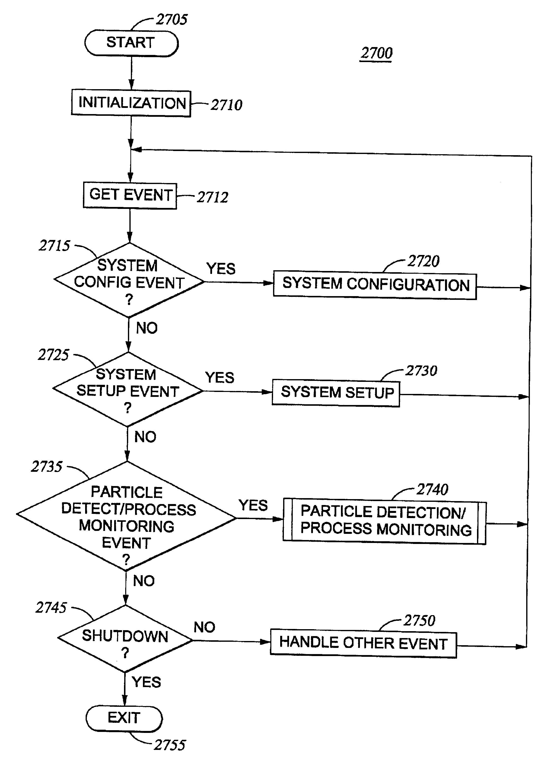
  • Figure 1
    Figure 1
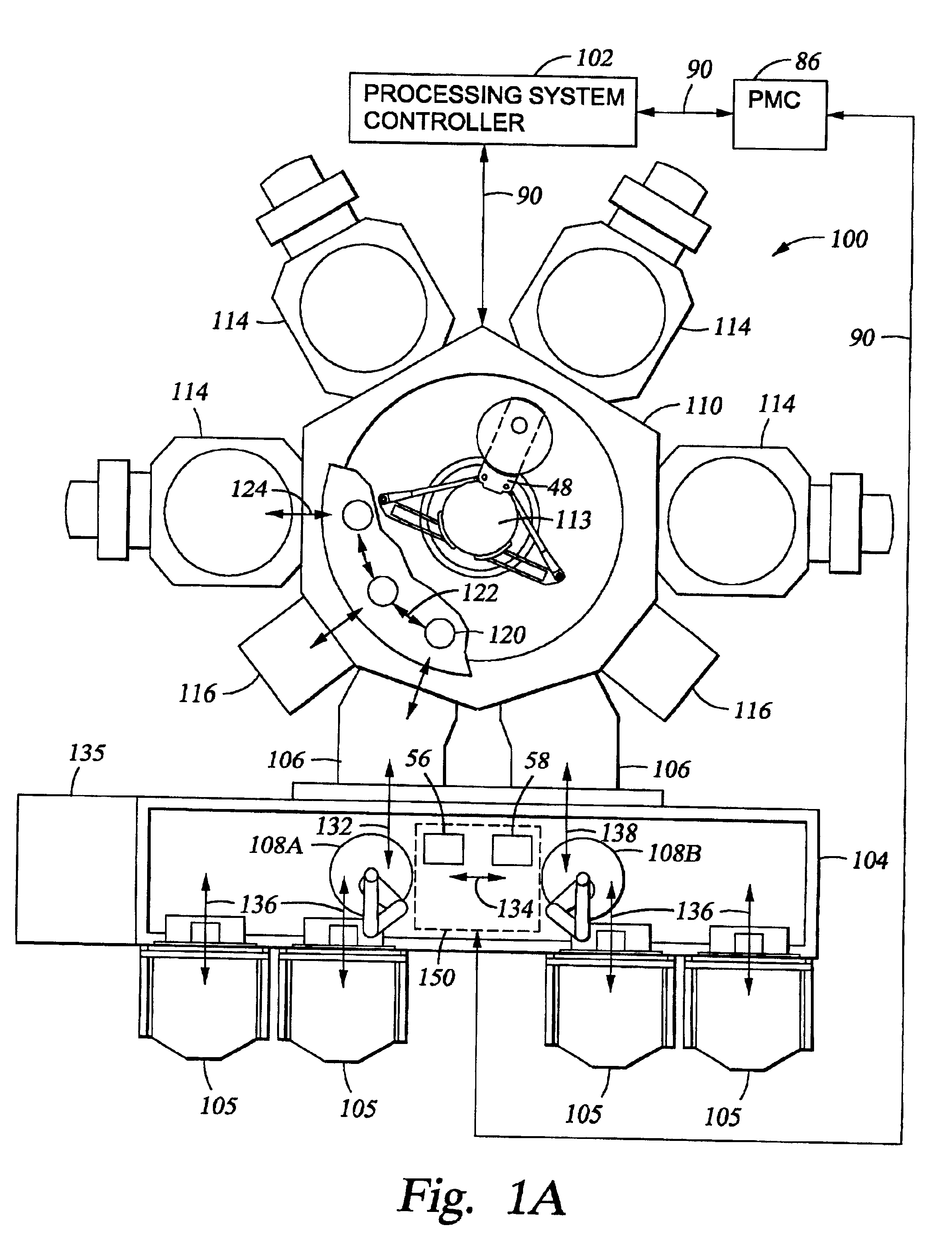
  • Figure 2
    Figure 2
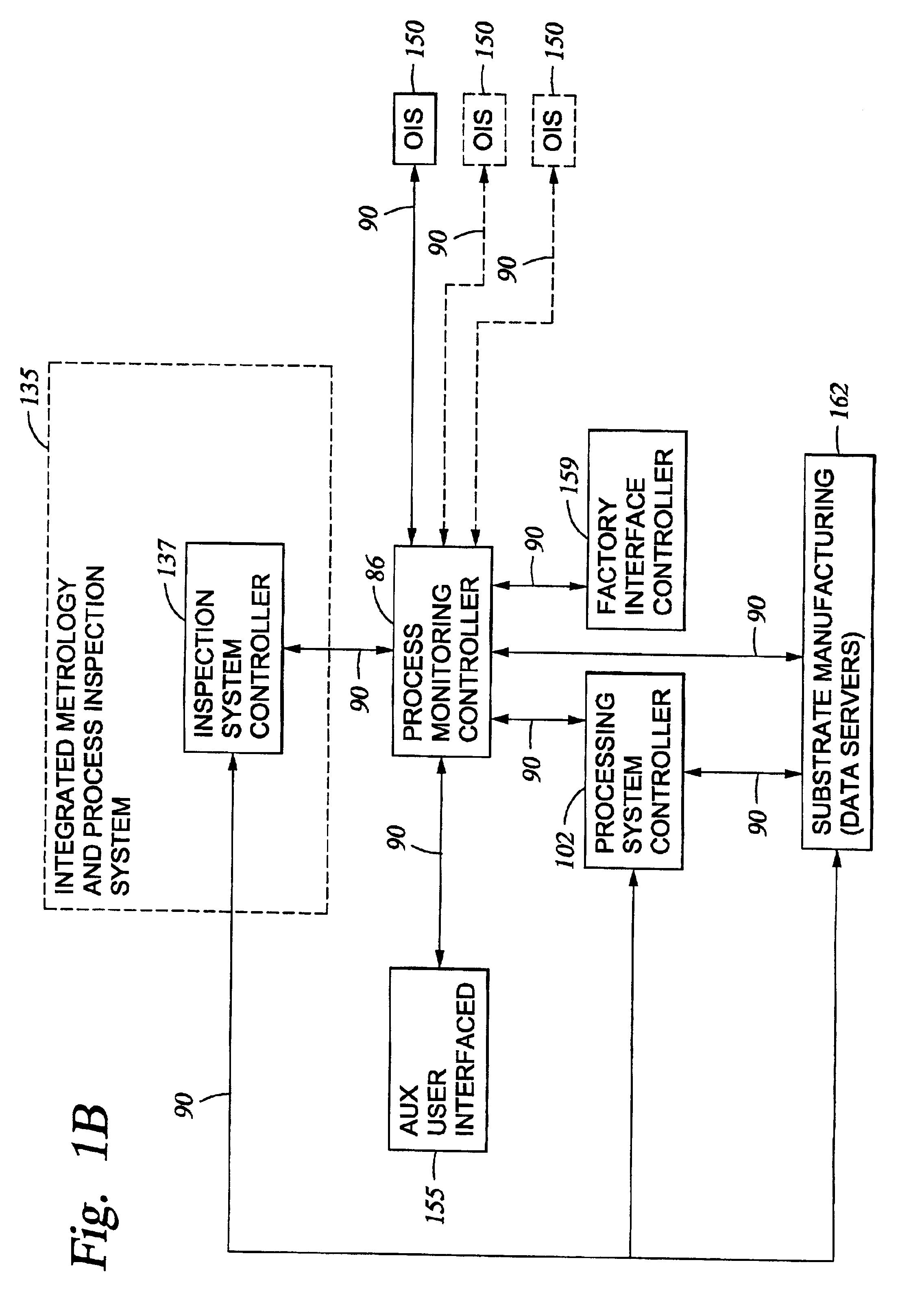
  • Figure 3
    Figure 3
Patent Text Reader

Abstract

The present invention generally provides an apparatus and a method for inspecting a substrate in a processing system. In one aspect, a light source is used in conjunction with an optical receiving device, such as a camera having a CCD, to illuminate and inspect a substrate for various optical signatures. The data collected during an inspection cycle is processed to determine substrate topography information. In one embodiment, the data is used to generate mean values indicative of signal intensity and / or color. One aspect provides for specular signature analysis where a reference histogram is subtracted from a test substrate histogram. The mean values are then compared to reference values to determine topographical conditions. Advantageously, a data processing system may be used to collect the data, perform the specular signature analysis, and determine the resultant processing conditions.
Need to check novelty before this filing date? Find Prior Art

Description

[0001] This application is a continuation-in-part of U.S. application Ser. No. 09 / 391,341 filed on Sep. 7, 1999, now U.S. Pat. No. 6,707,544, entitled “Particle Detection and Embedded Vision System to Enhance Substrate Yield and Throughput”BACKGROUND OF THE INVENTION

[0002] 1. Field of the Invention

[0003] The invention relates to inspection methods and apparatus. More particularly, the invention relates to a method and apparatus for inspection of substrates to identify process and handling related defects and conditions.

[0004] 2. Background of the Related Art

[0005] A chip manufacturing facility is composed of a broad spectrum of technologies. Cassettes containing semiconductor substrates are routed to various stations in the facility where they are either processed or inspected.

[0006] Semiconductor processing generally involves the deposition of material onto and removal (“etching”) of material from substrates. Typical processes include chemical vapor deposition (CVD), physical vapor depos...

Examples

example

[0146]Substrates were processed on a Centura system equipped with a DPS Metal Etch Chamber and an ASP strip / passivation chamber, both available from Applied Materials, Inc., located in Santa Clara, Calif. After etch and strip processing, this hot substrate is cooled to near room temperature in a cooldown chamber which includes an apparatus system according to an embodiment of the invention.

[0147]Processed substrates consisted of EPIC-generated substrates, utilizing Applied Materials equipment for all steps except for lithography. The photoresist / metal stack on the substrates was: 8000A DUV photoresist / 250A TiN ARCI5500A Al-Cu0.5% / 250A TiN / 200A Ti / 3000A thermal oxide. A dense pattern covered about 50% of the substrate, consisting of 0.25 μm lines / spaces.

[0148]All substrates were etched using a typical recipe. This etched the metal stack entirely, leaving approximately 5200A of photoresist on most patterned features (3700A at the shoulder of patterned lines).

[0149]As chip geometries s...