
Convergent charged particle beam apparatus and inspection method using same

a technology of charged particle beam and apparatus, applied in the direction of optical radiation measurement, instruments, therapy, etc., can solve the problems of deterioration in electron beam image quality, degradation of performance in comparison inspection or critical-dimension measurement, and inability to achieve correctness

Inactive Publication Date: 2005-04-26
HITACHI LTD
View PDF15 Cites 11 Cited by
  • Summary
  • Abstract
  • Description
  • Claims
  • Application Information

AI Technical Summary

Benefits of technology

[0016]It is therefore an object of the present invention to provide an arrangement for detecting a surface height of an object item in an observation / fabrication region of charged particle beam optics or in its vicinity under vacuum at high speed without causing interference with the charged particle beam optics.
[0017]According to the present invention, there is provided a highly reliable system in which the object item can be observed / fabricated with its image being always in focus using surface height data thus detected.

Problems solved by technology

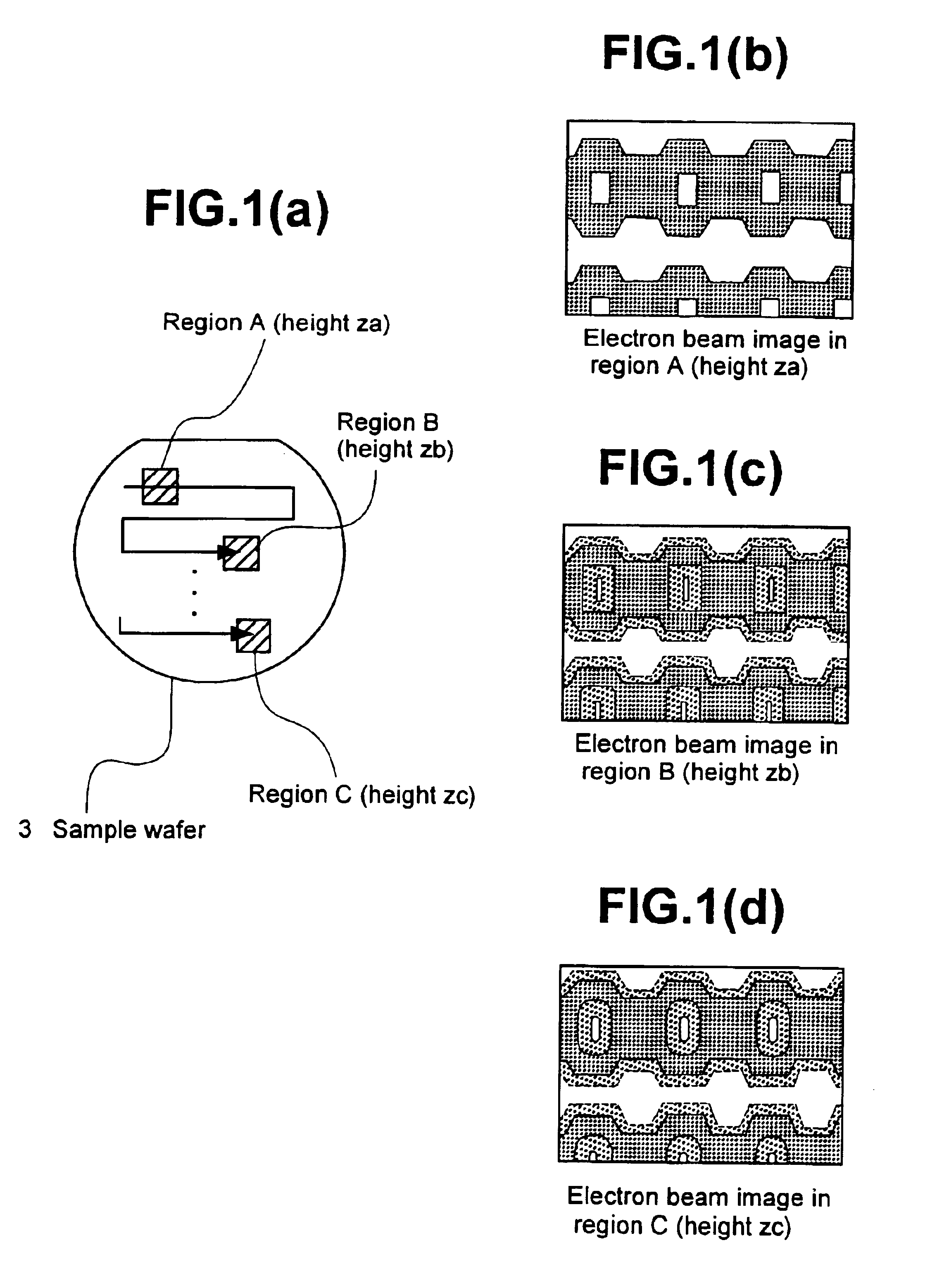
Deterioration in electron beam image quality occurs due to image distortion caused by deflection or aberration in electron optics, decreased resolution caused by defocusing, etc., resulting in degradation of performance in comparison inspection or critical-dimension measurement.
1(d), it is impossible to attain correct results.
Further, since these images provide variation in pattern dimensions and results of edge detection on them are unstable, pattern line widths and hole diameters cannot be measured accurately.
This procedure requires a substantial amount of time and involves repetitive scanning on a surface of a specimen, which may cause a possible problem of specimen damage.
However, this method is also disadvantageous in that a considerable amount of time is required for measuring an optimum objective lens control current before inspection and each specimen surface height may vary during inspection depending on wafer holding conditions.
However, since an optical element for height detection is disposed in a vacuum system, it is rather difficult to perform optical axis alignment.
In a scanning electron microscope, a method of measuring an optimum control current to an objective lens thereof through electron beam imaging necessitates attaining a plurality of electron beam images for detecting a focal point, thus requiring a considerable amount of time for focus adjustment.
That is, such a method is not suitable for focusing in a short time.
However, it is extremely difficult to hold the specimen wafer stably without causing interference with electron optics in a vacuum specimen chamber, and also it is impossible to adjust specimen leveling as in an optical inspection system using vacuum chucking.
Further, since a substantial amount of time is required for inspection, a specimen holding state may vary due to acceleration / deceleration in reciprocating stage movement, thereby resulting in a specimen surface height being different from a pre-measured level.
It is impossible to conduct focus adjustment continuously while detecting a height at each point simultaneously with stage movement for the specimen under inspection.
This causes a significant decrease in throughput as a size of wafer becomes larger.
Depending on the material of a specimen, exposure with an electron beam may alter an electric charge state on specimen surface to cause an adverse effect on electron beam images used for inspection.
In consideration of the above, it is difficult to ensure satisfactory performance in long-period inspection on a scanning electron microscope instrument using the conventional methods.
However, if any element which affects an electric or magnetic field, e.g., an insulating or magnetic element, is disposed in the vicinity of an observation region, electron beam scanning is affected adversely.

Method used


Image

  • Convergent charged particle beam apparatus and inspection method using same
  • Convergent charged particle beam apparatus and inspection method using same
  • Convergent charged particle beam apparatus and inspection method using same

Examples


Embodiment Construction

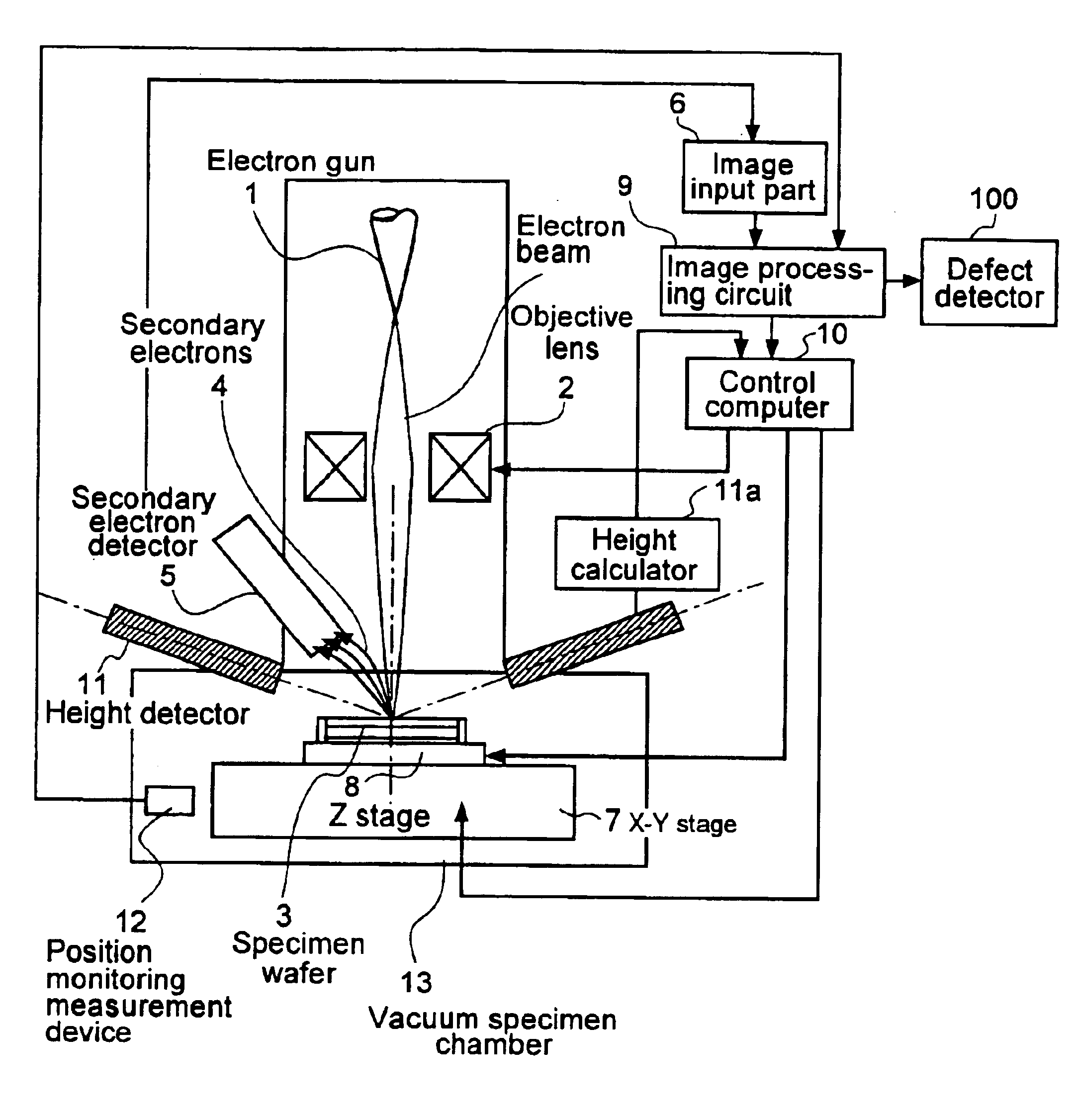
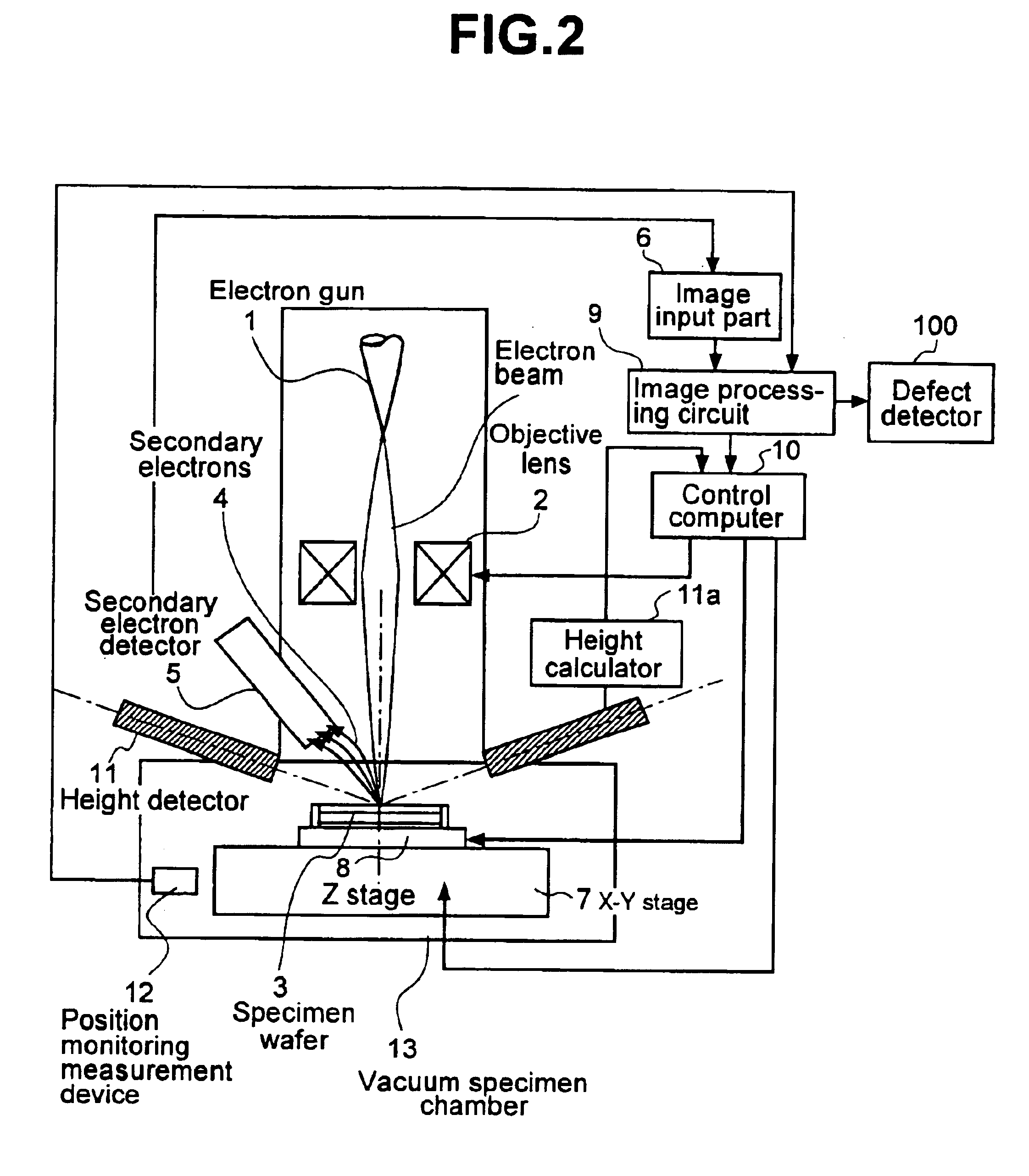
[0056]Referring now to the accompanying drawings wherein like reference numerals are utilized to designate like parts throughout the views, there is shown in FIG. 2 an overview of an automatic semiconductor device inspection system using electron beam images as an exemplary preferred embodiment of the present invention. In an electron optical system shown in FIG. 2, an electron beam emitted from an electron gun 1 is converged through an objective lens 2, and the electron beam thus converged can be scanned over a surface of a specimen in an arbitrary sequence. A signal of secondary electrons 4 produced on a surface of a specimen wafer 3 in irradiation with the electron beam is detected by a secondary electron detector 5, and then the secondary electron signal is fed to an image input part 6 as an image signal.

[0057]The specimen wafer under inspection can be moved by an X-Y stage 7 and a Z stage 8. By moving each stage, an arbitrary point on the surface of the specimen wafer is observ...


PUM


Abstract

A convergent charged particle beam apparatus includes an electron beam system which emits a converged electron beam, a vacuum chamber which is connected to the electron beam system, and a stage which mounts a specimen and moves at least in one direction inside of the vacuum chamber. An electron beam image observation unit observes an electron beam image of a surface of the specimen. A height detector optically detects a height of the specimen mounted on the stage by illuminating the surface of said specimen with light and by detecting reflected light of the illumination reflected from the surface of the specimen, and a controller controls a focus position of the electron beam in accordance with an output from the height detector while the stage is moving at least in one direction.

Description

CROSS REFERENCE TO RELATED APPLICATION[0001]This application a continuation application of U.S. application Ser. No. 10 / 426,702, filed May 1, 2003, now U.S. Pat. No. 6,744,057, which is a continuation of U.S. application Ser. No. 10 / 012,400, filed Dec. 12, 2001, now U.S. Pat. No. 6,559,459, which is a continuation of U.S. application Ser. No. 09 / 258,461, filed Feb. 26, 1999, now U.S. Pat. No. 6,335,532, which is a continuation-in-part application of U.S. application Ser. No. 09 / 132,220, filed Aug. 11, 1998, by some of the inventors herein, now U.S. Pat. No. 6,107,637, the subject matter of the aforementioned applications being incorporated by reference herein.BACKGROUND OF THE INVENTION[0002]The present invention relates to a convergent charged particle beam apparatus using a charged particle beam such as an electron beam or ion beam for microstructure fabrication or observation and an inspection method using the same, and more particularly to an automatic focusing system and arrang...

Claims


Application Information

Patent Timeline
IPC IPC(8): H01J37/02H01J37/21G01N1/28G01Q30/16G01Q30/20G01Q40/00G01Q60/44
CPCH01J37/21G01N2001/2893H01J2237/304H01J2237/2817
Inventor TANAKA, MAKIWATANABE, MASAHIROHIROI, TAKASHISHINADA, HIROYUKININOMIYA, TAKU
Owner HITACHI LTD
Learn More