Scalable LED with improved current spreading structures

a current spreading structure and led technology, applied in the field of light-emitting diodes, can solve the problems of insufficient light conversion efficiency of filament lights, limited size of conventional nitride-based leds, and limited use, so as to improve the light-emitting efficiency, improve the current spreading, and increase the power output and luminous flux.

Inactive Publication Date: 2005-04-26
CREE INC
View PDF10 Cites 114 Cited by
  • Summary
  • Abstract
  • Description
  • Claims
  • Application Information

AI Technical Summary

Benefits of technology

[0016]The present invention provides an improved LED with new current spreading structures. The improved LED can be standard sized or scaled to larger sizes, allowing for increased power output and luminous flux. Its new current spreading structures provide improve...

Problems solved by technology

One disadvantage of most conventional LEDs is that they are less efficient at converting current to light than are filament lights.
As a result, their use has most often been limited to applications such as indicating lamps in electronic devices, where the LED's die size is less than 0.25 mm and where optical power is less than 10 milliwatts (mW).
However, the size of conventional nitride based LEDs is limited by the inability of current to effectively spread from the electrical contacts to the active layer.
P-type nitride based semiconductor materials have relatively poor conductivity, and current applied to the p-type contact will only spread to a limited area within the p-type layer.
The current will not migrate to the entire active layer, and the LED can experience local heating and premature degradation around the contact.
As a result, the size of nitride base LEDs is limited by the both the p- and n-type layers' current spreading characteristics.
The substrate is very thick compared to the epitaxial layers and as a result, the overall current spreading into the active region is limited by the spreading provided by the p-type contact.
This basic structure is effective for small LEDs (approximately 0.25 ...

Method used


Image

  • Scalable LED with improved current spreading structures
  • Scalable LED with improved current spreading structures
  • Scalable LED with improved current spreading structures

Examples


Embodiment Construction

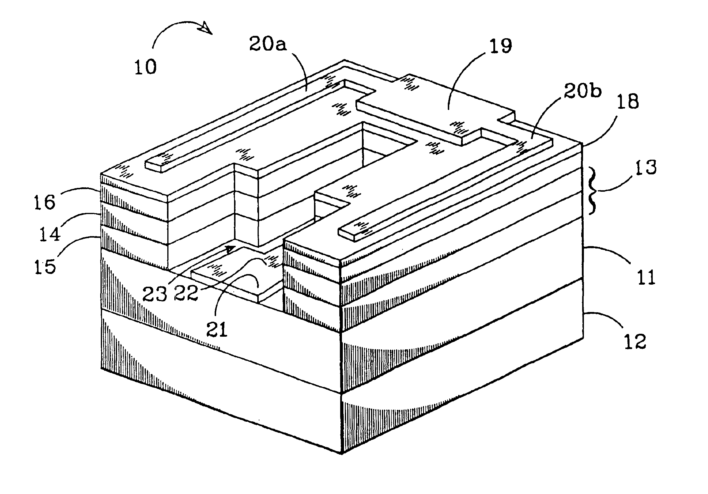
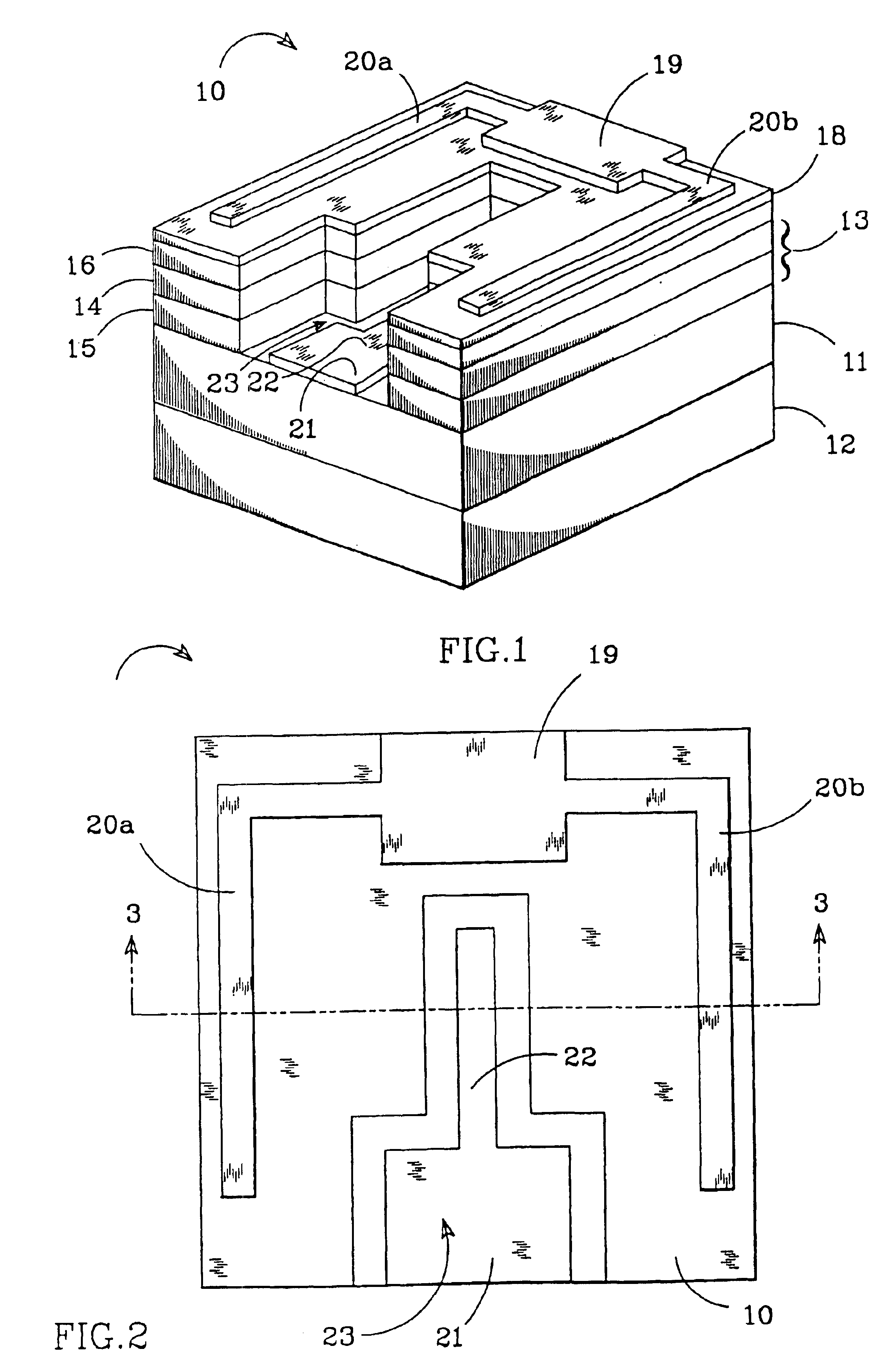
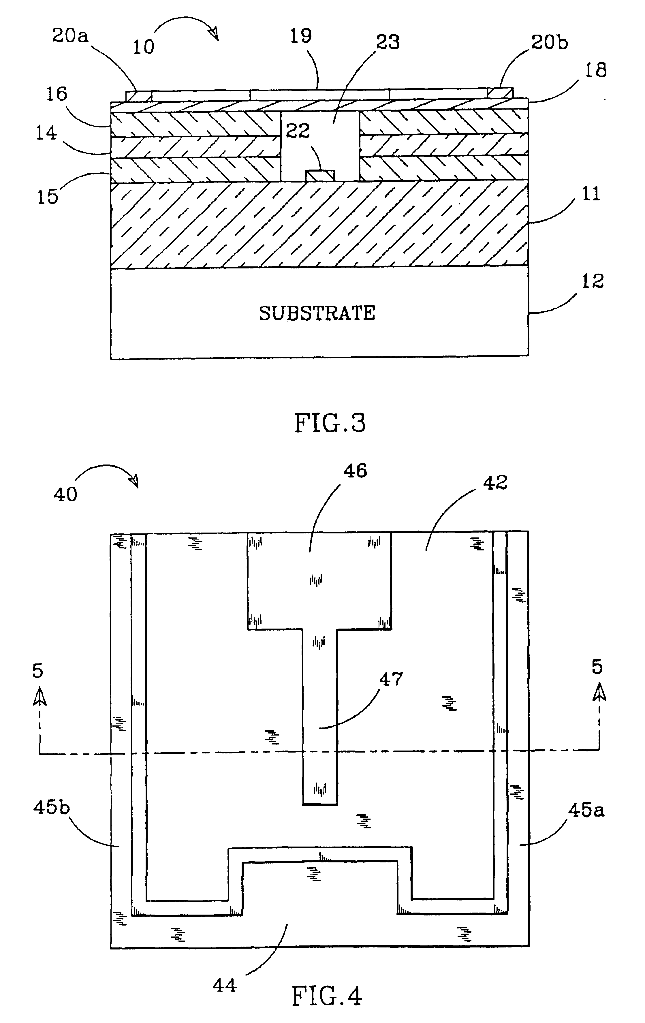
[0036]FIGS. 1-12 show various embodiments of a new LEDs constructed in accordance with the present invention, each having improved current spreading structures. The new structures can be used in LEDs formed from any semiconductor material system, but are particularly applicable to Group-III nitride based LEDs fabricated on substrates such as silicon carbide (SiC) or sapphire. SiC has a much closer crystal lattice match to Group III nitrides such as GaN and results in Group III nitride films of high quality. Silicon carbide also has a very high thermal conductivity so that the total output power of Group III nitride devices on silicon carbide is not limited by the thermal dissipation of the substrate (as is the case with some devices formed on sapphire). SiC substrates are available from Cree Research, Inc., of Durham, N.C. and methods for producing them are set forth in the scientific literature as well as in a U.S. Pat. Nos. Re. 34,861; U.S. Pat. No. 4,946,547; and U.S. Pat. No. 5,...


PUM


Abstract

An LED with improved current spreading structures that provide enhanced current injection into the LED's active layer, improving its power and luminous flux. The current spreading structures can be used in LEDs larger than conventional LEDs while maintaining the enhanced current injection. The invention is particularly applicable to LEDs having insulating substrates but can also reduce the series resistance of LEDs having conductive substrates. The improved structures comprise conductive fingers that form cooperating conductive paths that ensure that current spreads from the p-type and n-type contacts into the fingers and uniformly spreads though the oppositely doped layers. The current then spreads to the active layer to uniformly inject electrons and holes throughout the active layer, which recombine to emit light.

Description

[0001]This application is a divisional of and claims priority to U.S. patent application Ser. No. 09 / 721,352, which was filed on Nov. 21, 2000 now U.S. Pat. No. 6,614,056.BACKGROUND OF THE INVENTION[0002]1. Field of the Invention[0003]The present invention relates to light emitting diodes (LEDs) and more particularly to LEDs having improved current spreading structures.[0004]2. Description of the Related Art[0005]LEDs are an important class of solid state devices that convert electric current to light. They generally comprise an active layer of semiconductor material sandwiched between two oppositely doped layers, one being p-type and the other being n-type. A drive current is applied across electrical contacts on the doped layers causing electrons and holes to be injected from the doped layers into the active layer. The electrons and holes then recombine to generate light that emits omnidirectionlly from the active layer and escapes from all surfaces of the LED.[0006]One disadvanta...

Claims


Application Information

Patent Timeline
IPC IPC(8): H01L33/00H01L33/14H01L33/20H01L33/38H01L33/64
CPCH01L33/38H01L33/20H01L33/14H01L33/64
Inventor TARSA, ERIC J.THIBEAULT, BRIANIBBETSON, JAMESMACK, MICHAEL
Owner CREE INC
Why Eureka
Try Eureka