Transistor-type ferroelectric nonvolatile memory element

a ferroelectric non-volatile memory element, transistor-type technology, applied in semiconductor devices, semiconductor/solid-state device details, capacitors, etc., can solve the problems of destroying data held at the time of reading out data, limiting the area, and reducing the use of electric current and electric power, so as to reduce the area of memory cells, shorten the channel length, and improve the effect of memory cell area

Inactive Publication Date: 2005-04-26
SEIKO NPC +1
View PDF9 Cites 17 Cited by
  • Summary
  • Abstract
  • Description
  • Claims
  • Application Information

AI Technical Summary

Benefits of technology

[0019]This invention, therefore, is to solve the above problem inherent in the prior art. It is an object of this invention to provide a transistor-type ferroelectric nonvolatile memory element which has a decreased memory cell area t...

Problems solved by technology

Therefore, this could become a so-called destructive readout in which the data held at the time of reading out the data is destroyed.
This is a fundamental problem that occurs since the memory of this structure does not comply with the scaling side like the DRAM.
Namely, there is a limitation on decreasing the area, electric current and electric power used therefor.
Further, the transistor-type ferroelectric memory maintains the FET turned on or off relying upon the polarization of the ferroelectric material, and does not permit the data to be destroyed by the reading operation on a low voltage.
Limitation, however, is imposed on decreasing the thickness of the gate-insulating layer I from the standpoint of breakdown voltage and leakage current.
The above conventional method, how...

Method used


Image

  • Transistor-type ferroelectric nonvolatile memory element
  • Transistor-type ferroelectric nonvolatile memory element
  • Transistor-type ferroelectric nonvolatile memory element

Examples


first embodiment

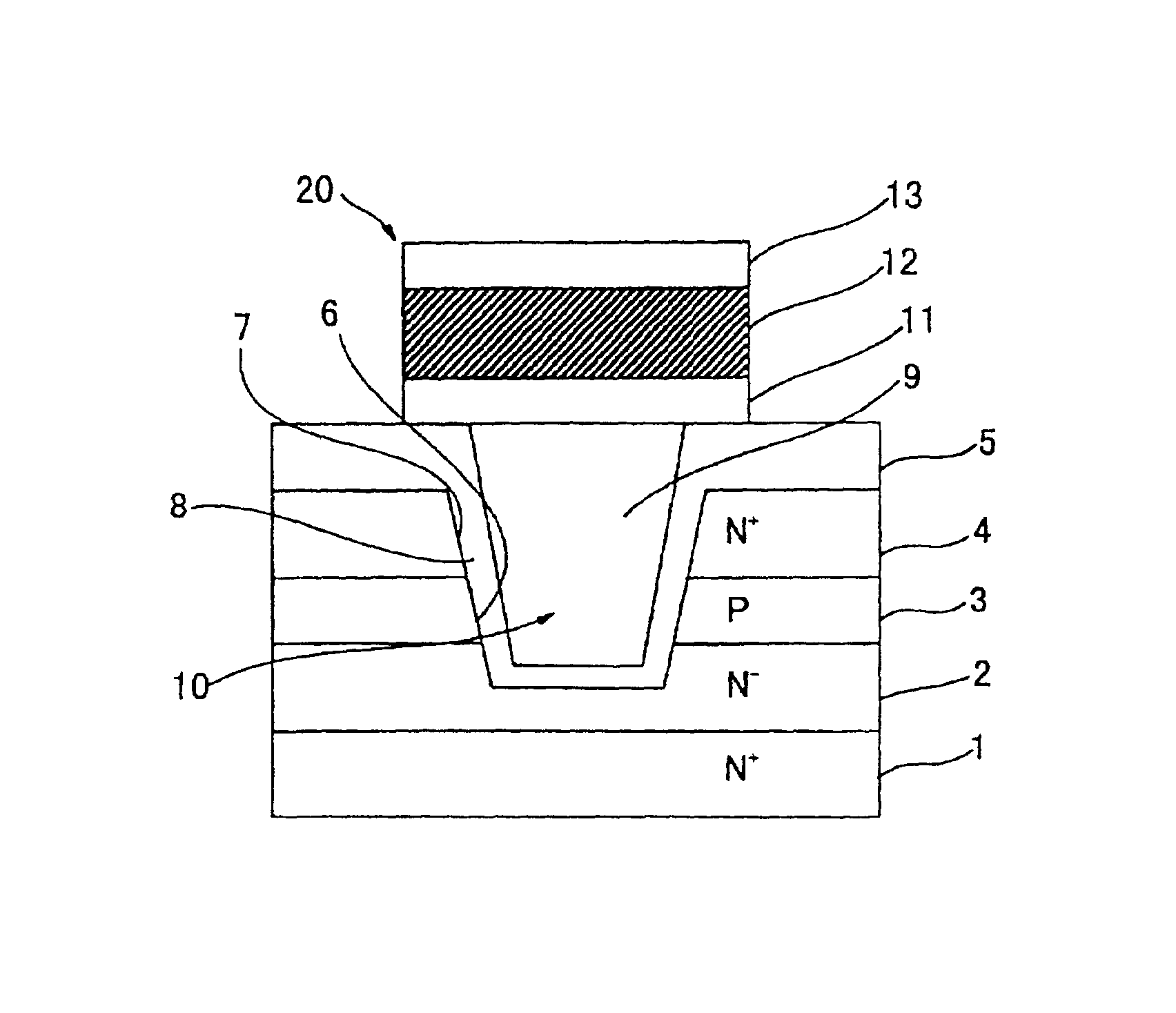
[0050]the present invention will be described with reference to FIG. 1. In this embodiment, an N−-type layer 2 is epitaxially grown on an N+-type silicon substrate (S) 1 that serves as a drain layer. In the N−-type layer 2 are doubly diffused P-type impurities and N-type impurities to successively form a P-type layer 3 that serves as a base layer and an N+-type layer 4 that serves as a source layer. An insulating layer 5 of silicon oxide is laminated on the N+-type layer 4 by the thermal oxidation. A trench 6 is formed in the substrate 1 reaching the N−-type layer 2 penetrating through the insulating layer 5, N+-type layer 4 and P-type layer 3. The trench 6 has side walls 7 that are inclined to some extent such that the opening portion thereof is slightly larger than the bottom portion thereof. The inner surfaces of the trench 6, i.e., the side surfaces and the bottom are covered with a silicon oxide film that serves as a gate oxide layer (I) 8.

[0051]The trench 6 is filled with, for...

third embodiment

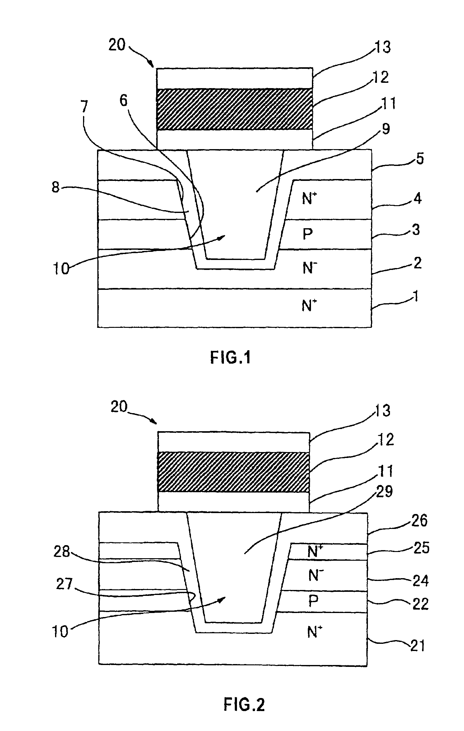
[0058]FIG. 3 illustrates the invention. This embodiment has a more simple MIS transistor structure 30. An N+-type layer 32 is formed by diffusion on a P-type silicon substrate 31. An insulating layer 33 of silicon oxide is laminated on the N+-type layer 32. A trench 34 is formed to reach the P-type silicon substrate 31 from the insulating layer 33 penetrating through the N′-type layer. The trench 34 divides the N+-type layer 32 into right and left parts, which constitute a drain region 35 and a source region 36, respectively. A gate oxide film 37 is formed on the inside of the side walls and bottom surface of the trench 34. The trench 34 is filled with a conductor 38 such as polycrystalline silicon to thereby form a MIS structure 30. An MFM structure 20 is formed on the flat trench 34 like in FIG. 1.

[0059]In the structure of the third embodiment of FIG. 3, too, the effective area of the capacitance of the MIS structure 30 is determined by the gate oxide film 37 on the inner surface ...

fourth embodiment

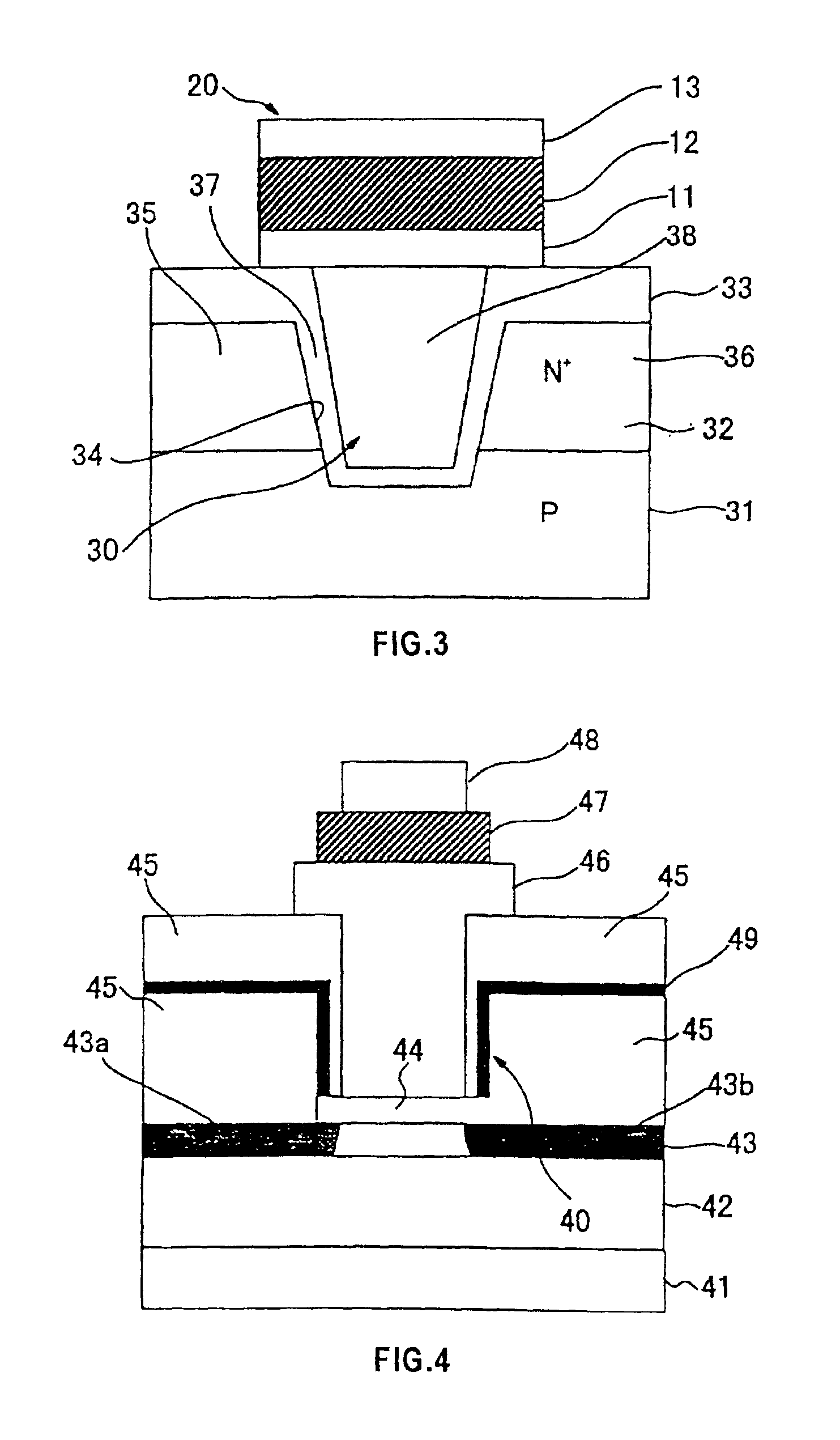
[0062]Next, described below with reference to FIG. 4 is this invention. This embodiment uses an SOI (silicon-on-insulator) substrate. If an MIS structure and an MFM structure are stacked on a thin SOI layer, then, it becomes difficult to form a deep silicon trench that was formed in the above embodiments. Therefore, an MIM (metal-insulator-metal) structure is formed between the MIS structure and the MFM structure to increase the effective area of the capacitance of the MIS structure. A region for forming a channel is constituted in the middle portion of the SOI layer 43, and a gate oxide film (I) 44 is laminated thereon.

[0063]That is, an insulating film 42 is laminated on a semiconductor substrate 41, and a semiconductor layer (S) 43 is laminated thereon. Both sides of the semiconductor layer 43 are forming a source region 43a and a drain region 43b, respectively. A region for forming a channel is constituted in the middle portion of the semiconductor layer 43, and a gate oxide film...


PUM


Abstract

A transistor-type ferroelectric nonvolatile memory element having an MFMIS (metal-ferroelectric-metal-insulator-semiconductor) structure that can be highly densely integrated. The MFMIS transistor has a constitution in which the MFM (metal-ferroelectric-metal) structure and the MIS (metal-insulator-semiconductor) structure are stacked up and down on nearly the same area, and the lower MIS structure has means for increasing the effective area of the MIS capacitance. Means for increasing the effective area of the capacitor is a trench in the semiconductor substrate, ruggedness in the MIS structure or a MIN (metal-insulator-metal) structure.

Description

BACKGROUND OF THE INVENTION[0001]1. Field of the Invention[0002]This invention relates generally to a nonvolatile memory element and, more specifically, to a transistor-type ferroelectric nonvolatile memory element by using a ferroelectric material as a control gate.[0003]2. Prior Art[0004]A ferroelectric memory which has now been put into practice has a constitution in which the capacitor of DRAM is replaced by a ferroelectric capacitor (see, for example, Japanese Unexamined Patent Publication (Kokai) No. 113496 / 1990). The operation is based upon the detection of a difference in the amount of electric charge between when the polarization of capacitance of the ferroelectric material is inverted and when it is not inverted, thereby to judge whether the stored data is [1] or [0]. Therefore, this could become a so-called destructive readout in which the data held at the time of reading out the data is destroyed.[0005]According to this method in which an electric charge by the inversion...

Claims


Application Information

Patent Timeline
IPC IPC(8): H01L21/02H01L27/115H01L21/28H01L29/66H01L29/78H01L21/8247H01L27/10H01L27/105H01L29/788H01L29/792
CPCH01L21/28291H01L29/78391H01L27/11502H01L28/55H01L29/40111H10B53/00H01L27/105
Inventor TARUI, YASUOSAKAMAKI, KAZUO
Owner SEIKO NPC
Why Eureka
Try Eureka