
Semiconductor device having at least three power terminals superposed on each other

a technology of power terminals and semiconductors, applied in semiconductor devices, semiconductor/solid-state device details, electrical apparatus, etc., can solve the problems of inconvenient self-inductance increase and wiring resistance caused by bonding wires b>64/b>, and achieve the effect of improving heat diffusion and reducing wiring resistan

Inactive Publication Date: 2005-04-26
KK TOSHIBA
View PDF13 Cites 26 Cited by
  • Summary
  • Abstract
  • Description
  • Claims
  • Application Information

AI Technical Summary

Benefits of technology

[0009]The present invention relates to a structure for reducing a wiring resistance caused by the wiring metal such as bonding wire, and self-inductance, and further improving the heat diffusion, and is a semiconductor device having at least three or more power terminals superimposed on each other, at least one semiconductor chip arranged in a way sandwiched between two predetermined power terminals among the power terminals, wherein the two power terminals and the semiconductor chip are connected electrically each other.
[0010]By providing such a configuration, it becomes possible to reduce considerably the voltage drop due to the internal wiring, because the connection between semiconductor chips and power terminals is realized by a short distance and through a surface. Also, in a case of adopting an array for flowing current mutually in the opposite direction in a way to reduce the inductance component of the external power terminal, it is possible to intend to reduce further by a mutual inductance.
[0011]Further, it is possible to realize a structure unnecessary to connect additionally a new another heat radiation plate, as the power terminals of both upper and lower ends and the relay power terminal function as heat radiation plate, allowing to intend to reduce the process load and to cut the cost. In addition, it is possible to make a structure not requiring an insulation substrate for wiring layout. Therefore, a low heat resistance can be realized, as it becomes unnecessary to use an insulation substrate of lower heat conductivity than the metal.

Problems solved by technology

Consequently, wiring resistance caused by the bonding wire 64 and self-inductance increase inconveniently.

Method used


Image

  • Semiconductor device having at least three power terminals superposed on each other
  • Semiconductor device having at least three power terminals superposed on each other
  • Semiconductor device having at least three power terminals superposed on each other

Examples


first embodiment

[0035](First Embodiment)

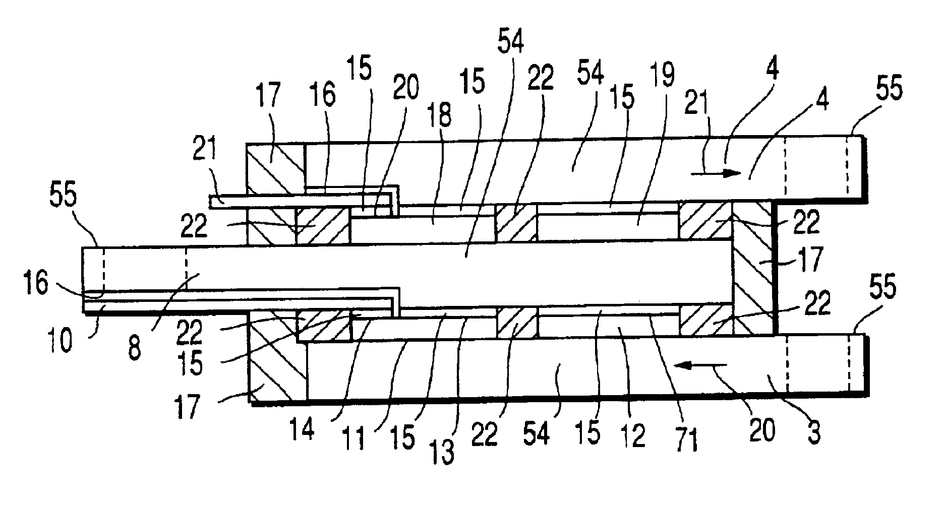
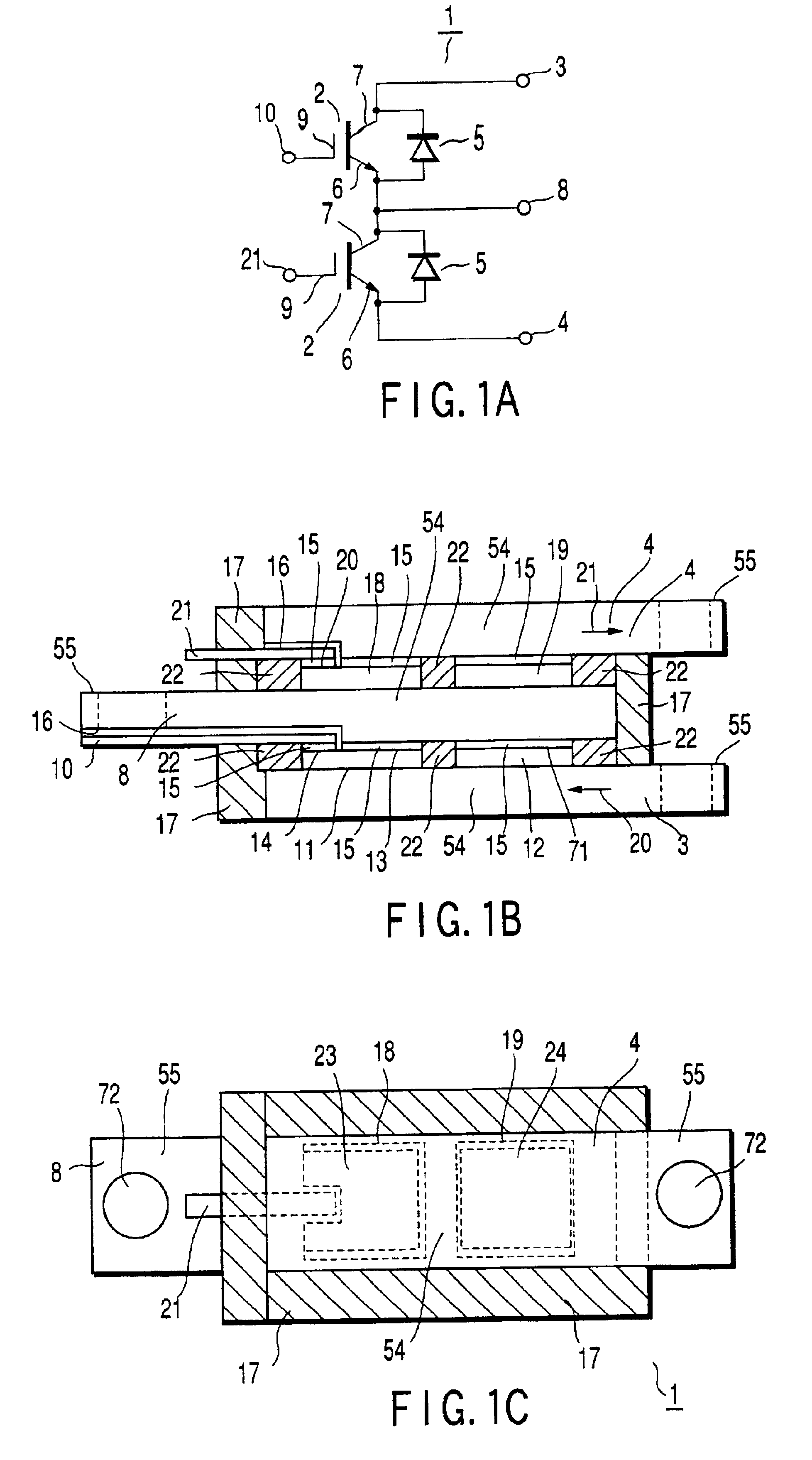
[0036]FIG. 1A shows a IGBT module 1 having a half bridge configuration, which is a first embodiment of the present invention. The a circuit diagram of this IGBT module 1 is shown in FIG. 1A, a schematic section view of this IGBT module is shown in FIG. 1B and a plan view showing the schematic configuration of this IGBT module inside is shown in FIG. 1C.

[0037]In the IGBT half bridge circuit shown in FIG. 1A, two IGBT elements 2 are connected in series and a collector 7 of one IGBT element and an emitter of the other IGBT element are connected respectively to a first and a second external power elements 3, 4. In addition, diodes 5 are connected respectively in parallel to the emitter 6 and the collector 7 of respective IGBT elements. A relay power terminal 8 which is third external power element is connected between two IGBT elements. Control terminals 10, 21 are connected respectively to a gate of two IGBT elements 2.

[0038]The structure of this IGBT module is ...

second embodiment

[0049](Second Embodiment)

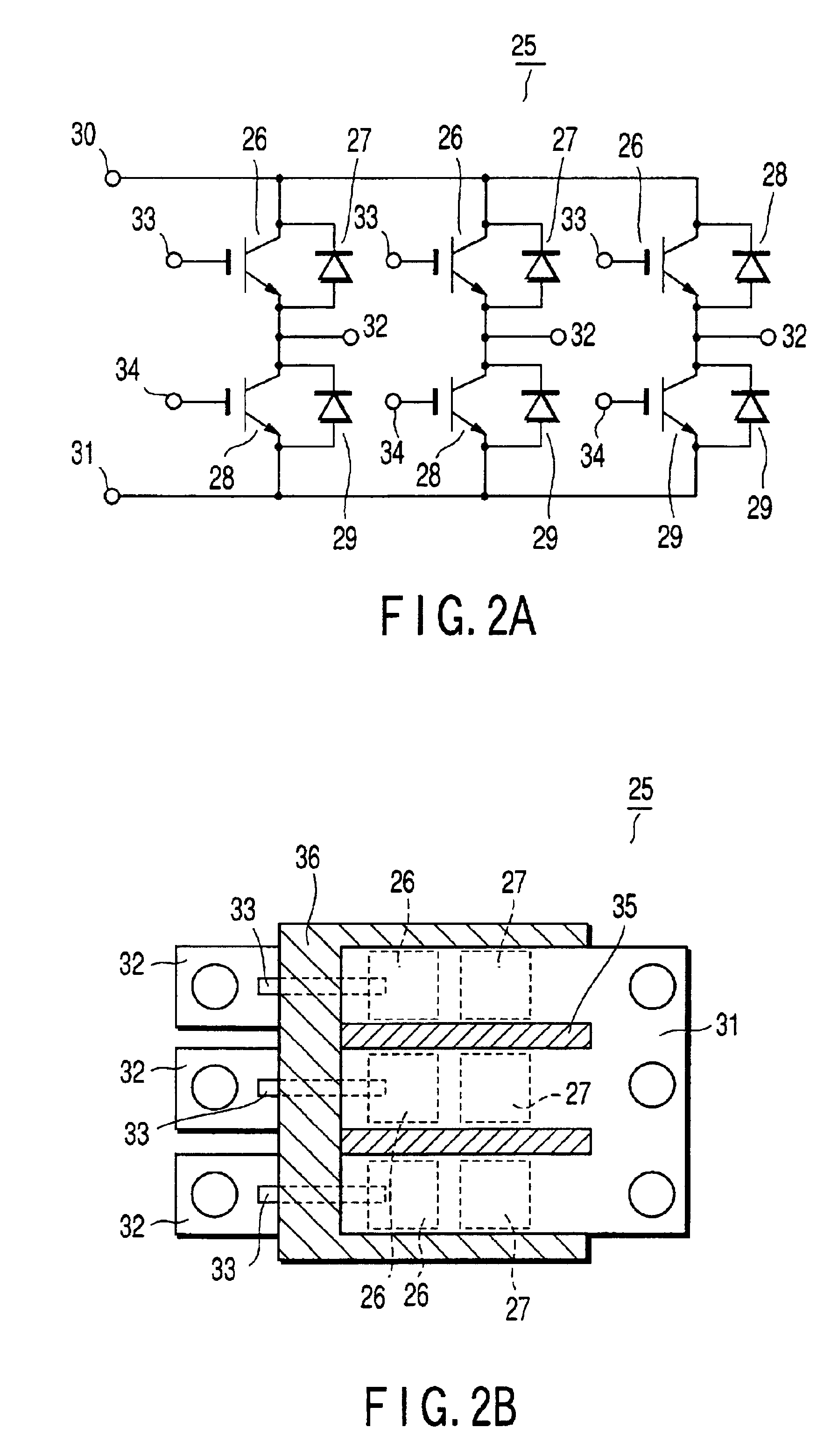
[0050]FIG. 2 shows an IGBT module 25 of 6in1 structure which is a second embodiment of the invention. Here, FIG. 2A shows the circuit diagram of an IGBT module, and FIG. 2B shows the module inside plan view.

[0051]In the second embodiment, a single module is constituted by connecting in parallel three circuits of IGBT module of the first embodiment. Three upper IGTB 26 are arranged on three lower IGBT 28, and upper and lower IGBT 26, 27 are connected respectively in series, forming a three phased structure. In addition, three upper diodes 27 are arranged on three lower diodes 29, and upper and lower diodes are connected in parallel respectively to the corresponding IGBT.

[0052]Respective phase is bound respectively to the first external power terminal 30 and the second external power terminal 31 integrating three phases. A relay power terminal 32 is formed at the junction of upper and lower elements of each phase, and control terminals 33, 34 to be connected t...

third embodiment

[0054](Third Embodiment)

[0055]FIG. 3 shows the inside plan view of a third embodiment modifying the structure of the control terminals 21, 10 and the second external power terminal 4 of the first embodiment. It is different from the first embodiment in that a structure for connecting an IGBT chip 37 and a control terminal 38 by a bonding wire 39 (or soldering) and taking out the control terminal 38 from the center of a module 40. As necessary, it is also possible to constitute to bring a signal system emitter terminal 41 near the control terminal 38 and to output directly from the external power terminal 4. Such a configuration makes easy to bound the control apparatus with the control system circuit, especially to dispose the wiring, in a case of using the IGBT module for power control apparatus or others.


PUM


Abstract

The present has an object of reducing a wiring resistance caused by the wiring metal such as bonding wire, and self-inductance, in a semiconductor device for large power, such as IGBT module. Therefore, the invention has at lest three or more power terminals superimposed on each other, wherein at least one semiconductor chip is connected electrically in a way to be sandwiched between predetermined two power terminals among the power terminals. A power terminal on one end among the aforementioned superposed power terminals and a power terminal on the other end among the superposed power terminals can be led out in the same direction, for example.

Description

CROSS-REFERENCE TO RELATED APPLICATIONS[0001]This application is based upon and claims the benefit of priority from the prior Japanese Patent Application No. 2000-210475, field Jul. 11, 2000, the entire contents of which are incorporated herein by reference.BACKGROUND OF THE INVENTION[0002]1. Field of the Invention[0003]The present invention relates to a semiconductor device for large power, such as IGBT module. Also, the invention is applied to the structure of semiconductor device required to reduce the power loss.[0004]2. Description of the Related Art[0005]A structure, as shown in FIG. 9 for instance, is known as an example of semiconductor device for large power according to the prior art. Here, this example relates to the structure of IGBT module.[0006]In FIG. 9A, a collector side of an IGBT chip 65 and an n layer side of a diode chip 66 are soldered respectively, on a Cu pattern 63 of the surface of a DBC (Direct Bond Copper) substrate wherein copper conductors sandwich an in...

Claims


Application Information

Patent Timeline
Patent Type & Authority Patents(United States)
IPC IPC(8): H01L25/07H01L25/18H01L25/16
CPCH01L25/071H01L25/18H01L2224/48091H01L2224/48137H01L2924/13055H01L2924/1301H01L2924/30107H01L2924/14H01L2924/13034H01L2224/48227H01L2224/32245H01L2924/00014H01L2924/00H01L2224/48139H01L25/07
Inventor HIRAHARA, FUMIOOGATA, KENICHI
Owner KK TOSHIBA
Learn More