

Method for fabricating semiconductor device
a technology of semiconductor devices and manufacturing methods, applied in the direction of semiconductor lasers, semiconductor laser structural details, lasers, etc., can solve the problems of difficult crystal growth of nitride semiconductors, difficult formation of nitride semiconductors, and crystal growth on the same substrate as that of epitaxial growth layers, etc., to achieve the effect of large surface area
- Summary
- Abstract
- Description
- Claims
- Application Information
AI Technical Summary
Benefits of technology
Problems solved by technology
Method used
Image

Examples
embodiment 1
[0055]A first embodiment of the present invention will be described with reference to the drawings.
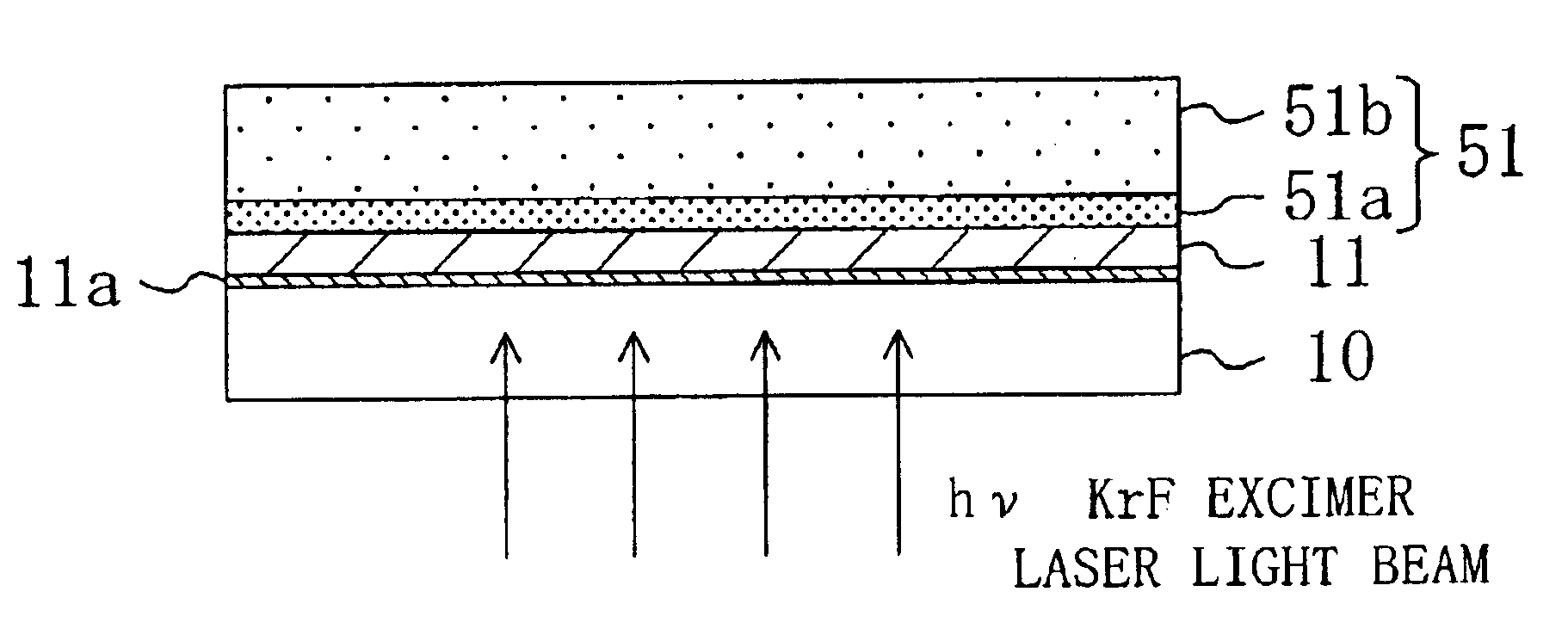
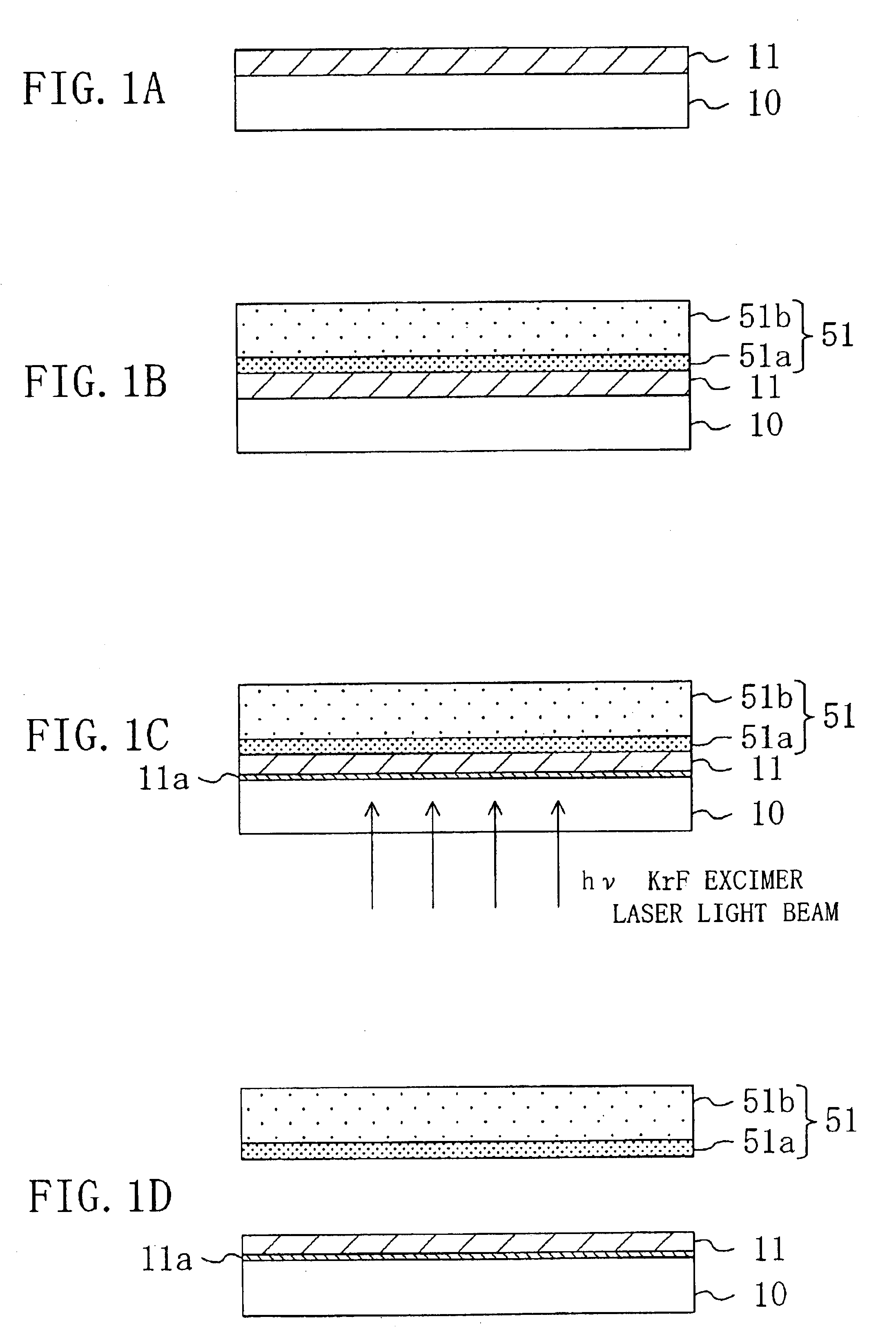
[0056]FIGS. 1A through 1D show cross-sectional structures in the order of procedure of a method for fabricating a semiconductor device according to the first embodiment.
[0057]The first embodiment is a method for producing a semiconductor layer (wafer) with a substrate for use in a semiconductor device such as a light-emitting diode.
[0058]First, as shown in FIG. 1A, a nitride semiconductor layer, i.e., a semiconductor layer 11 of InxGayAl1-x-yN (where 0≦x, y≦1 and 0≦x+y≦1), is grown by, for example, a metal organic chemical vapor deposition (MOCVD) process to a thickness of about 3 μm on a sapphire substrate (wafer) 10 at a growth temperature of about 1000° C. In this case, in order to make the crystallinity of the semiconductor layer 11 excellent, the semiconductor layer 11 may be grown after a so-called low-temperature buffer layer (not shown) of aluminum nitride (AlN) or gallium nitr...
embodiment 2
[0071]A second embodiment of the present invention will be described with reference to the drawings.
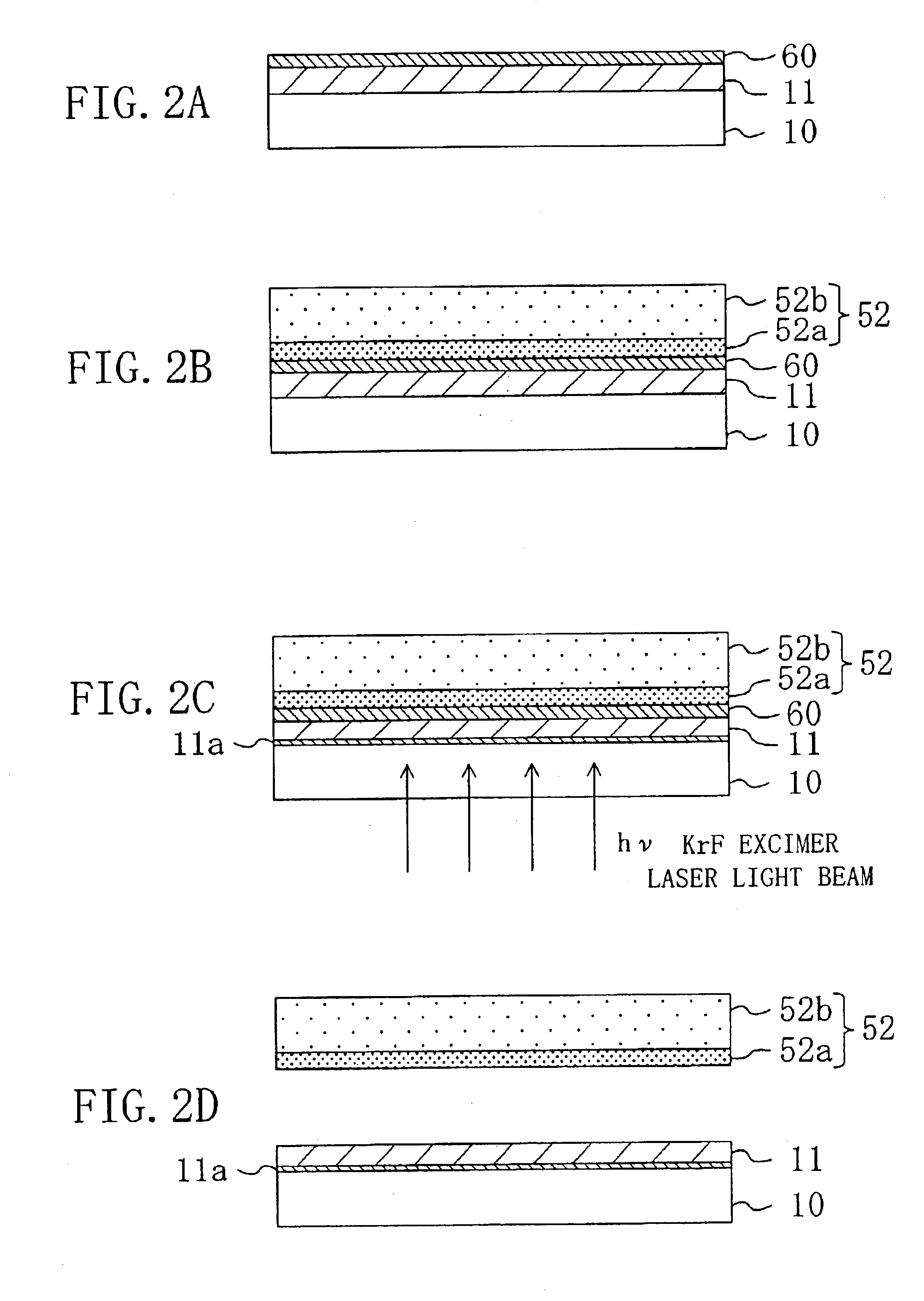
[0072]FIGS. 2A through 2D show cross-sectional structures in the order of procedure of a method for fabricating a semiconductor device according to the second embodiment.
[0073]The second embodiment is a method for producing a semiconductor layer (wafer) with a substrate for use in a semiconductor device such as a light-emitting diode.
[0074]First, as shown in FIG. 2A, a nitride semiconductor layer, i.e., a semiconductor layer 11 of InxGayAl1-x-yN (where 0≦x, y≦1 and 0≦x+y≦1), is grown by, for example, an MOCVD process to a thickness of about 3 μm on a sapphire substrate 10 (wafer) at a growth temperature of about 1000° C. In this case, in order to make the crystallinity of the semiconductor layer 11 excellent, the semiconductor layer 11 may be grown after a low-temperature buffer layer (not shown) of aluminum nitride or gallium nitride has been grown to a thickness of about 50 nm at a ...
embodiment 3
[0085]A third embodiment of the present invention will be described with reference to the drawings.
[0086]The third embodiment is a method for fabricating a semiconductor device such as a light-emitting diode or a semiconductor laser.
[0087]FIGS. 3A through 3E show cross-sectional structures in the order of procedure of a method for fabricating a semiconductor device according to the third embodiment.
[0088]First, as shown in FIG. 3A, an n-type nitride semiconductor layer, i.e., a first semiconductor layer 21 of n-type InxGayAl1-x-yN (where 0≦x, y≦1 and 0≦x+y≦1), is grown by, for example, an MOCVD process to a thickness of about 4 μm on a sapphire substrate (wafer) 10 at a growth temperature of about 1000° C. In this case, in order to make the crystallinity of the first semiconductor layer 21 excellent, the first semiconductor layer 21 may be grown after a low-temperature buffer layer (not shown) of aluminum nitride or gallium nitride has been grown to a thickness of about 50 nm at a g...
PUM
 Abstract
Description
Claims
Application Information