Method for modifying resist images by electron beam exposure

Inactive Publication Date: 2005-05-31
ELECTRON VISION CORP
View PDF4 Cites 27 Cited by
  • Summary
  • Abstract
  • Description
  • Claims
  • Application Information

AI Technical Summary

Problems solved by technology

However the resolution capacity that can be obtained with conventional deep UV microlithography has its limits.
The deep UV photoresist materials that are used today, however, are not suitable for 157 nm, 193 nm and 248 nm exposure.
Materials based on phenolic resins as a binding agent, particularly novolak resins or polyhydroxystyrene derivatives have too high an absorption at wavelengths and one cannot image through films of the necessary thickness.
This high absorption results in side walls of the developed resist structures which do not form the desired vertical profiles.
Rather they have an oblique angle with the substrate which causes poor optical resolution characteristics at these short wavelengths.
However, in many cases they lack either sufficient etch resistance, thermal stability, post exposure delay stability, and/or processing latitude.
While such photoresists are sufficiently transparent for deep uv radiation, they do not have the etching stability customary for resists based on phenolic resins for plasma etching.
This leads to an improvement in etching stability, but not to the desired extent.
The use of metal-containing reagents, however, is generally not desired in microlithography process, due to the danger associated with contamination of the substrate with metal ions.
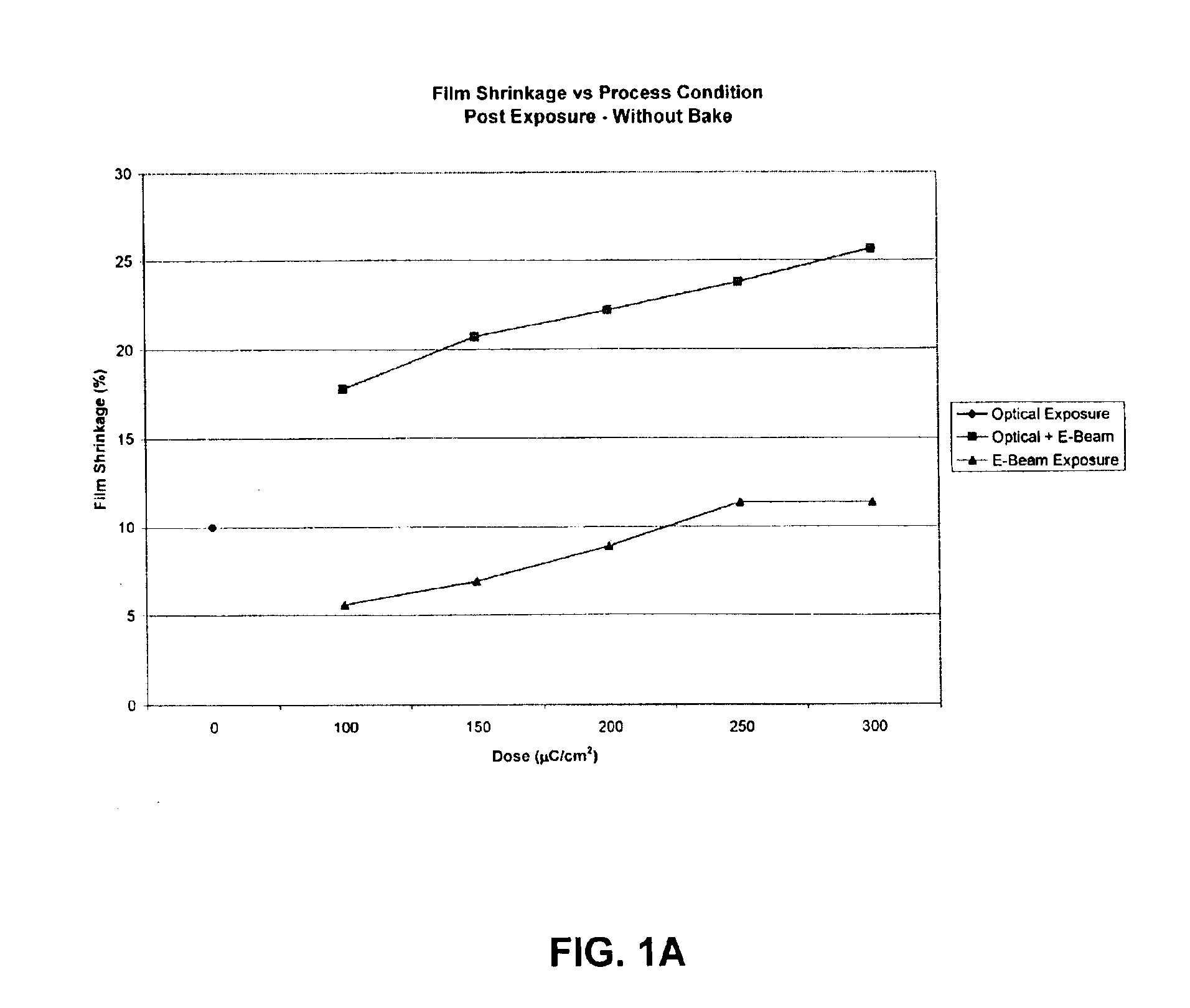
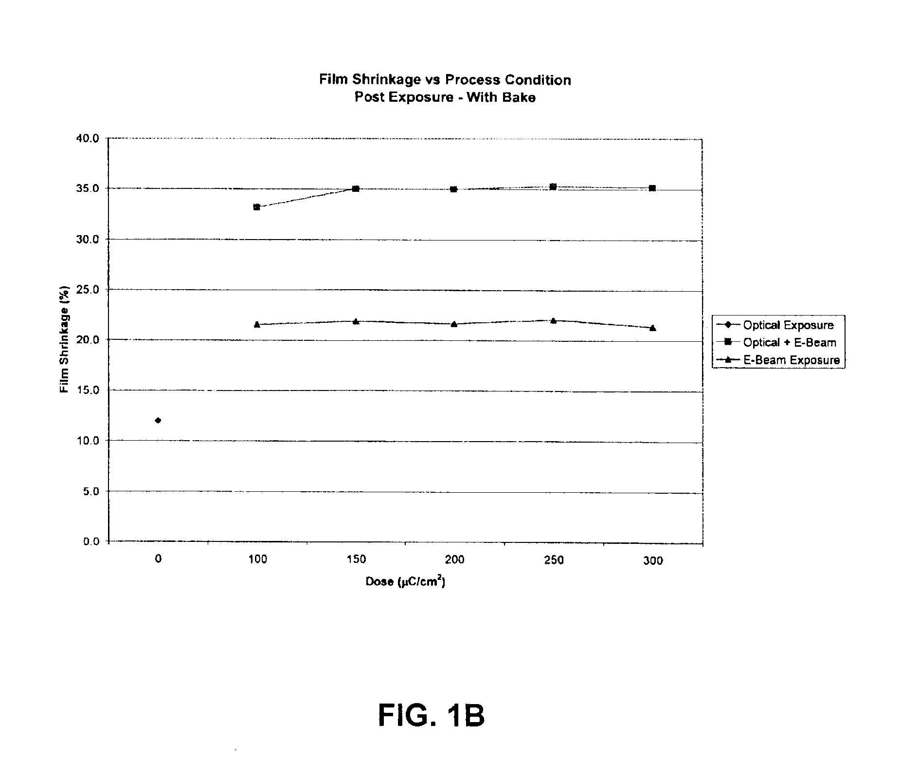
Due to the volatility of the additives in these resist materials, electron beam exposure causes the expulsion of these additives, which causes shrinking of the resist.
These are usually very large, or bulky, molecules that are attached to the resin via bonds that

Method used


Image

  • Method for modifying resist images by electron beam exposure
  • Method for modifying resist images by electron beam exposure
  • Method for modifying resist images by electron beam exposure

Examples


example 1

[0068]A set of ten 100 mm Silicon wafers were prepared by spin coating and baking a chemically amplified resist according to the manufacturer's recommended process. The resist for this example is PAR-101A4 from Sumitomo Chemical of Osaka, Japan. The resist was spin coated on a bench top spin-coat system from Laurell Technologies. The resist was post apply baked (PAB) at 130° C. for 60 seconds per the manufacturer's recommended processing conditions. This resulted in a resist film thickness of approximately 4000 Å. This set of ten wafers was then split into two groups of five wafers each.

[0069]The resist was then optically exposed using a Pen-Ray lamp with emission bands at 2540 Å and 1893 Å across one-half of the wafer. The exposure time was 10 seconds for all wafers. A separate set of tests determined that 10 seconds was sufficient to expose the resist and allow for complete development of the material. No mask was used to create patterns for the following tests. The resist was the...


PUM


Abstract

It has now been surprisingly found that by exposing a photoresist to flood electron beam exposure in combination with optical exposure, that the pullback on the upper region of lithographic images in resist can be virtually eliminated during electron beam processing. This unexpected result is due to the fact that the electron beam exposure and optional bake are carried out prior to development of the resist. This means that the resist shrinkage that is seen as a result of these steps is constrained laterally by the resist film itself. Thus, the resist is free to shrink vertically, and the resulting shrinkage provides a reduction in the line slimming and an improvement in the etch rate of the resist. This leads to the formation of a better resist image.

Description

BACKGROUND OF THE INVENTION[0001]1. Field of Invention[0002]The present invention relates to a method for modifying photoresist images, which are suitable for use in the production of electronic devices such as integrated circuits. More particularly, the invention provides a method for modifying photoresist images by applying a flood electron beam exposure to the resist in combination with optical exposure or patterning.[0003]2. Description of the Related Art[0004]The production of photoresists is well known in the art as exemplified by U.S. Pat. Nos. 3,666,473; 4,115,128 and 4,173,470. These contain aqueous alkali soluble polyvinyl phenol or phenol formaldehyde novolak resins together with light sensitive materials, usually a substituted naphthoquinone diazide compound. The resins and sensitizers are dissolved in an organic solvent and are applied as a thin film coating to a substrate suitable for the particular application desired. The resin component of photoresist formulations i...

Claims


Application Information

Patent Timeline
IPC IPC(8): G03F7/40G03F7/38G03F7/20
CPCG03F7/38G03F7/2022
Inventor LIVESAY, WILLIAM R.ROSS, MATTHEW F.
Owner ELECTRON VISION CORP
Why Eureka
Try Eureka