Shielded planar capacitor

Active Publication Date: 2005-06-07
TEXAS INSTR INC
View PDF11 Cites 67 Cited by
  • Summary
  • Abstract
  • Description
  • Claims
  • Application Information

AI Technical Summary

Benefits of technology

[0016]Electrical connections to the plates of the capacitor stack are provided by conductive vias attached to the plates extending through respective openings in the isolation layers and through slots or other such openings in the shield layers. Such slots in the shield layers also mitigate eddy current losses in the capacitor plates or shield layers that would otherwise develop in solid or continuous conductive layers.
[0017]The invention provides for more predictable planar capacitor performance that reduces stray capacitance and unwanted coupling by shielding the capacitor stack within a fully enclosed Faraday cage. The invention further a

Problems solved by technology

These delays may be related to stray parasitic capacitances between adjacent metal lines and/or semiconductor components as well as the resistance of interconnect metal lines through the multi-layer interconnect networks.
Some integrated circuits and integrated circuit devices are particularly sensitive to stray capacitances and noise, such as those components at the inputs of operational amplifiers and other similar high input impedance or high gain circuits, high speed switching circuits, or radio frequency (RF) integra

Method used


Image

  • Shielded planar capacitor
  • Shielded planar capacitor
  • Shielded planar capacitor

Examples


Embodiment Construction

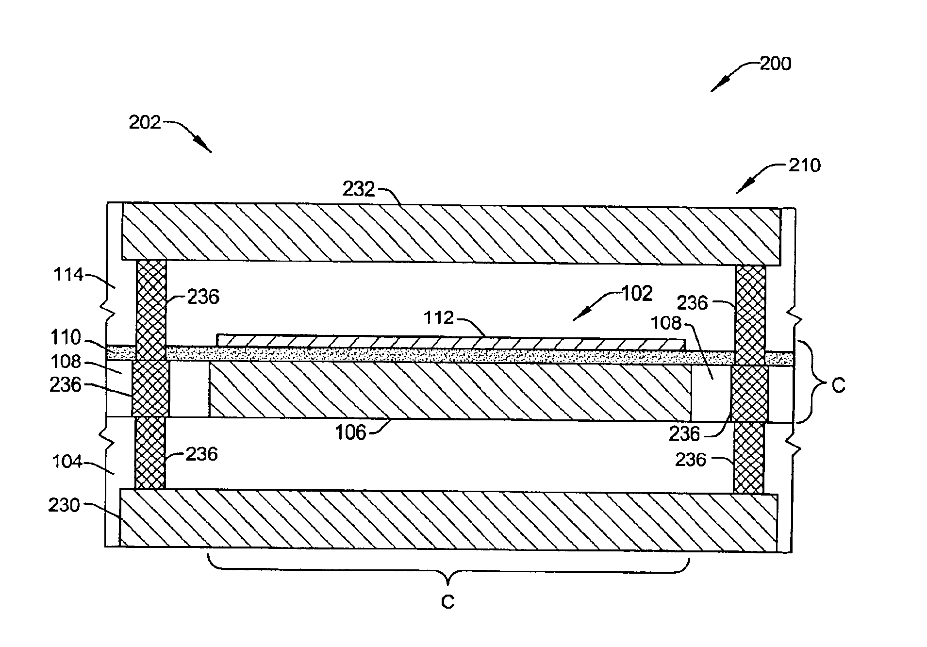
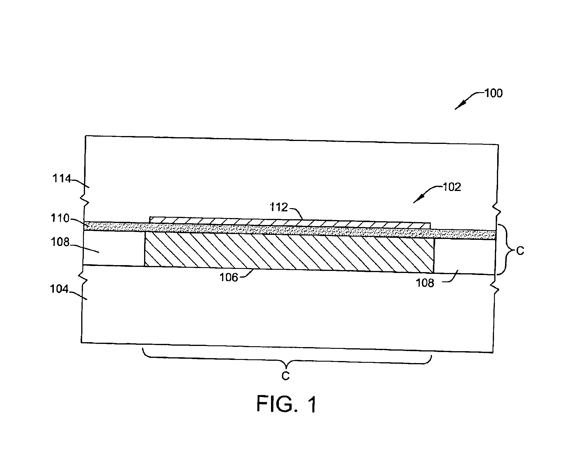
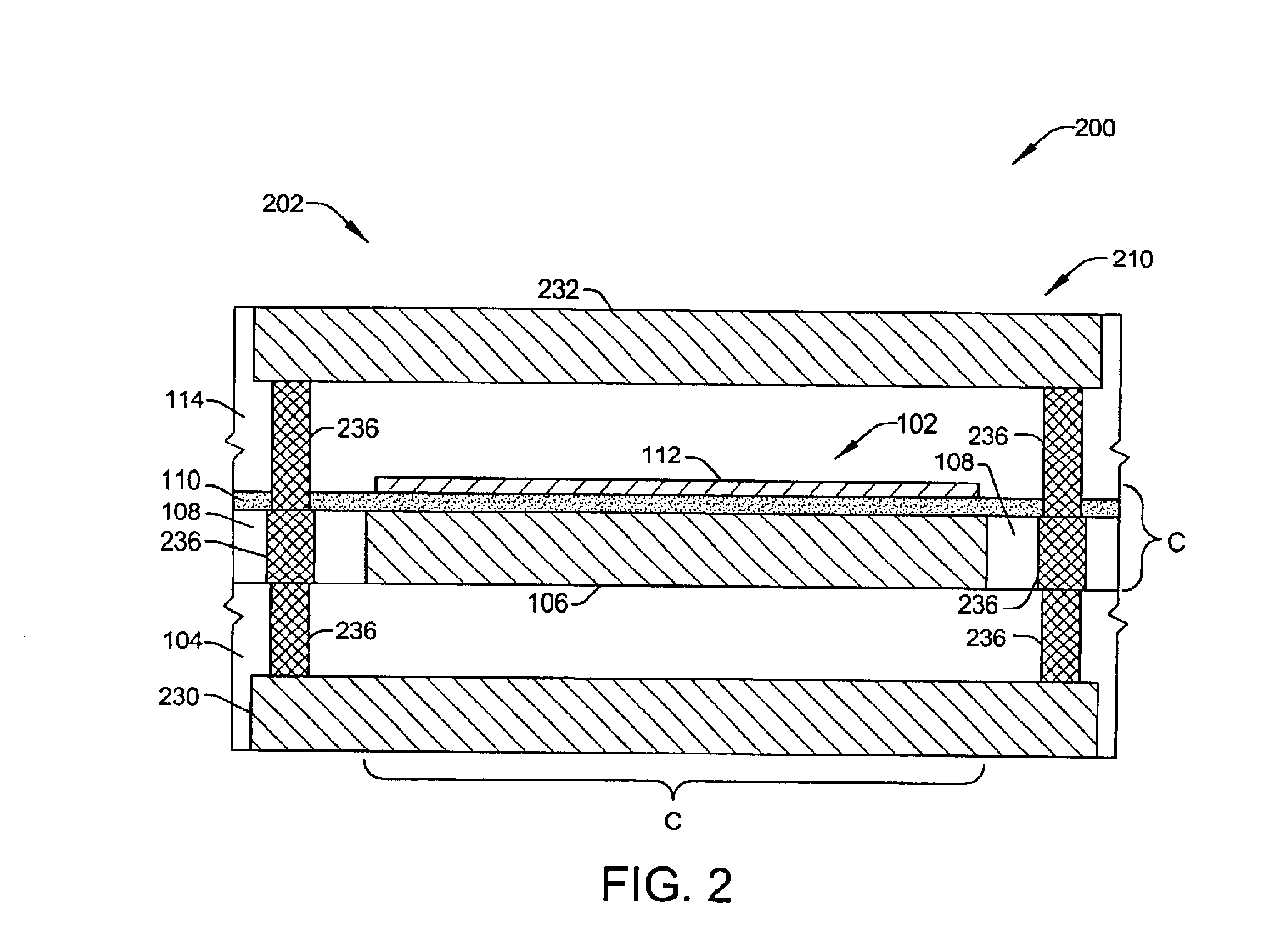
[0024]The present invention will now be described with reference to the attached drawings, wherein like reference numerals are used to refer to like elements throughout. The invention relates to a shielded planar capacitor formed within an enclosed Faraday cage during interconnect metal level processing of integrated circuits and other devices. One or more implementations of the invention are hereinafter illustrated and described in the context of the formation of the planar capacitor and the Faraday cage in semiconductor devices, utilizing etch-stop layers, isolation layers, tantalum, and interconnect metal layers. However, it will be appreciated by those skilled in the art that the invention is not limited to the exemplary implementations illustrated and described hereinafter. In particular, a variety of such materials may be used to form the structures discussed.

[0025]As previously indicated, because of increasing device densities and operational speeds, reduction of the delay ti...


PUM


Abstract

A shielded planar capacitor structure (202) is discussed, formed within a Faraday cage (210) in an integrated circuit device (200). The capacitor structure (202) reduces parasitic capacitances within the integrated circuit device (200). The capacitor (202) comprises a capacitor stack (102) formed between a first and second metal layers (230,232) of the integrated circuit. The capacitor stack (102) has a first conductive layer formed from a third metal layer (106) disposed between the first and second metal layers (230,232) of the integrated circuit, a dielectric isolation layer (110) disposed upon the first conductive layer (106); and a second conductive layer (112) disposed upon the dielectric isolation layer (110) and overlying the first conductive layer (106). The structure (202) further has a first and second isolation layers (104,114) disposed upon opposite sides of the capacitor stack (102). The Faraday cage (210) is formed between the first and second metal layers (230,232) of the integrated circuit (200), comprising a first and second shield layers (402,414) each having a plurality of mutually electrically conductive spaced apart traces (404). The first and second isolation layers (404,414) and the capacitor stack (102,434) are sandwiched between the first and second shield layers (402,414). Conductive elements (432) are distributed around the periphery of the capacitor stack (102,434) and the first and second isolation layers (404,412). The conductive traces (424) of the first shield layer (402) are connected to the conductive traces (424) of the second shield layer (414) through the conductive elements (432).

Description

FIELD OF INVENTION[0001]The present invention relates generally to semiconductor devices and more particularly to a planar capacitor shielded from noise and parasitic capacitances by a Faraday cage formed within the interconnect layers in the fabrication of integrated circuit devices.BACKGROUND OF THE INVENTION[0002]In the manufacture of semiconductor products such as integrated circuits, individual electrical devices are formed on or in a semiconductor substrate, and are thereafter interconnected to form circuits. Interconnection of these devices within an integrated circuit is typically accomplished by forming a multi-level interconnect network in layers formed over the electrical devices, by which the device active elements are connected to other devices to create the desired circuits. Individual wiring layers within the multi-level network are formed by depositing an insulating or dielectric layer over the discrete devices or over a previous interconnect layer, and patterning an...

Claims


Application Information

Patent Timeline
IPC IPC(8): H01G4/228
CPCH01G4/228H01L23/5223H01L28/87H01L23/5225H01L2924/3011H01L2924/0002H01L2924/00
Inventor BRENNAN, KENNETH D.
Owner TEXAS INSTR INC
Why Eureka
Try Eureka