Multilayer printed wiring board and method for producing multilayer printed wiring board

a technology of printed wiring board and multi-layer printing, which is applied in the direction of printed circuit aspects, printed circuit non-printed electric components association, printed circuit components, etc., can solve problems such as ic chip reliability degradation, ic chip eroded, and printed circuit board to ic chip cut off or cause malfunctions

Inactive Publication Date: 2005-06-21
IBIDEN CO LTD
View PDF19 Cites 142 Cited by
  • Summary
  • Abstract
  • Description
  • Claims
  • Application Information

AI Technical Summary

Problems solved by technology

These lead members tend to be cut off and eroded, making the connection of the printed circuit board to the IC chip cut off or causing malfunctions.
However, if bubbles are contained at the time of filling the resin, then the lead members are broken, the IC pads are eroded and reliability of the IC chip is deteriorated due to the bubbles.
Further, in case of employing a thermosetting resin, it is necessary to select a thermosetting resin in view of the materials of the lead members, a solder resist and the like, thereby disadvantageously causing cost increase..
First, if the die pad becomes fine pitch and small in size, alignment at the time of forming via holes becomes difficult.
On the other hand, if laser is applied and the via diameter is larger than the diameter of the die pad, a polyimide layer (or protective layer of the IC) is damaged by the laser.
Moreover, if the die pad of the IC chip is very small and the diameter of the via is larger than the size of the die pad, then positioning becomes quite difficult even by photo-etching or laser and connection errors occur between the die pad and the via hole.
Further, ceramic cannot be used for the substrate since it is inferior in outside workability.
It is difficult to form a conductive metallic film having a thickness exceeding

Method used


Image

  • Multilayer printed wiring board and method for producing multilayer printed wiring board
  • Multilayer printed wiring board and method for producing multilayer printed wiring board
  • Multilayer printed wiring board and method for producing multilayer printed wiring board

Examples


first embodiment

[First Embodiment]

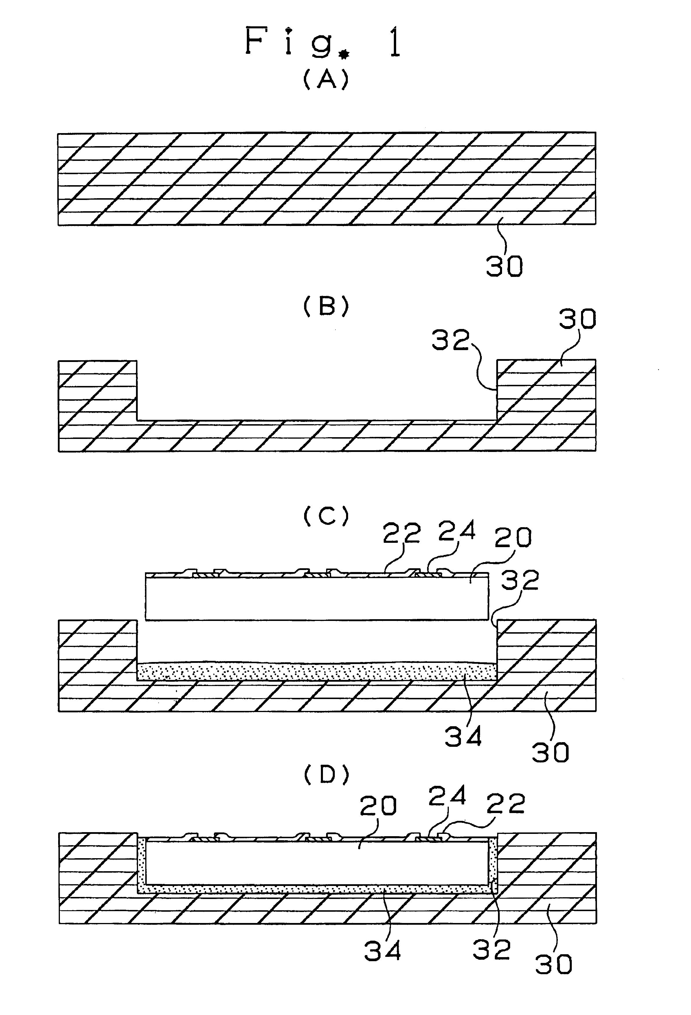
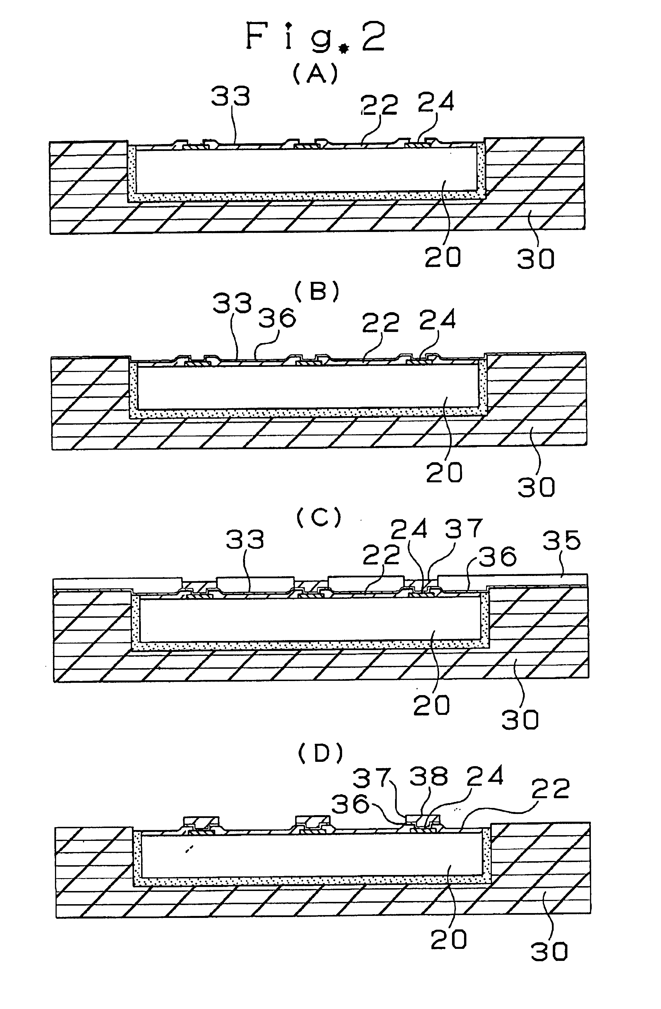
[0099]First, the constitution of a multilayer printed circuit board according to the first embodiment of the present invention will be described with reference to FIG. 6 showing the cross-sectional view of a multilayer printed circuit board 10.

[0100]As shown in FIG. 6, the multilayer printed circuit board 10 consists of a core substrate 30 containing therein an IC chip 20, an interlayer resin insulating layer 50 and an interlayer resin insulating layer 150. Via holes 60 and conductor circuits 58 are formed on the interlayer resin insulating layer 50. Via holes 160 and conductor circuits 158 are formed on the interlayer resin insulating layer 150.

[0101]The IC chip 20 is covered with a passivation film 22 and die pads 24 each constituting an input / output terminal are provided in the openings of the passivation film 22. A transition layer 38 is formed on each die pad 24 made of aluminum. The transition layer 38 consists of three layers of the first thin film layer 33,...

second embodiment

[Second Embodiment]

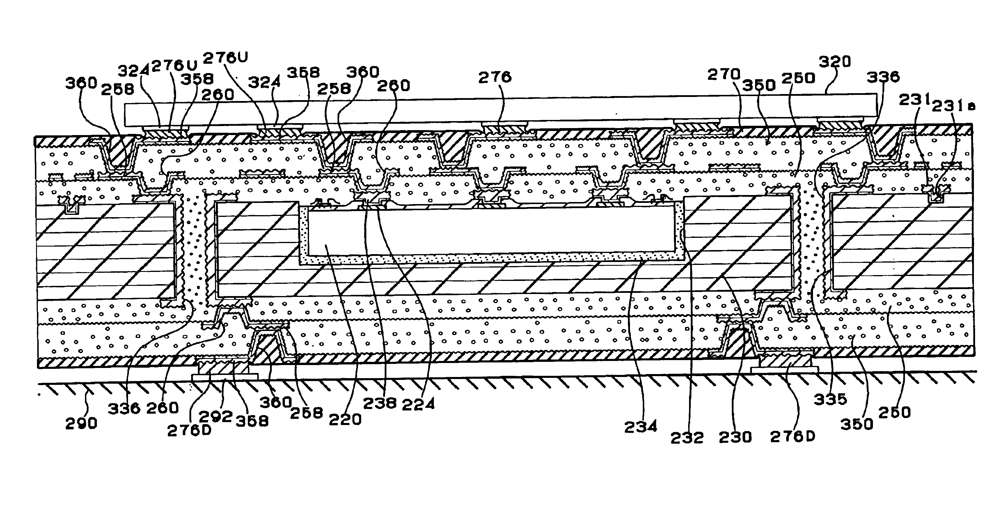
[0169]Next, the constitution of a multilayer printed circuit boar according to the second embodiment of the present invention will be described with reference to FIG. 18 showing the cross-section of a multilayer printed circuit board 210.

[0170]As shown in FIG. 18, the multilayer printed circuit board 210 consists of a core substrate 230 containing therein an IC chip 220, an interlayer resin insulating layer 250 and an interlayer resin insulating layer 350. Via holes 260 and conductor circuits 258 are formed on the interlayer resin insulating layer 250. Via holes 360 and conductor circuits 358 are formed on the interlayer resin insulating layer 350.

[0171]The IC chip 220 is covered with a passivation film 222, and die pads 224 each constituting an input / output terminal and positioning marks 223 are provided in the respective openings of the passivation film 222. A transition layer 238 mainly consisting of copper is formed on each die pad 224.

[0172]A solder resist la...

third embodiment

[Third Embodiment]

[0202]Next, the constitution of a multilayer printed circuit board according to the third embodiment of the present invention will be described hereinafter with reference to FIG. 26 showing the cross section of a multilayer printed circuit board 410.

[0203]As shown in FIG. 26, the multilayer printed circuit board 410 consists of a core substrate 430 containing therein an IC chip 420, an interlayer resin insulating layer 450 and an interlayer resin insulating layer 550. Via holes 460 and conductor circuits 458 are formed on the interlayer resin insulating layer 450. Via holes 560 and conductor circuits 558 are formed on the interlayer resin insulating layer 550.

[0204]The IC chip 420 is covered with an IC protective film (made of passivation+polyimide) 422 and aluminum die pads 424 each constituting an input / output terminal are provided in the respective openings of the IC protective film 422. An oxide film 426 is formed on each die pad 424. A transition layer 43 B is...


PUM

PropertyMeasurementUnit
Areaaaaaaaaaaa
Dissociation constantaaaaaaaaaa

Abstract

A multilayer printed circuit board has an IC chip 20 included in a core substrate 30 in advance and a transition layer 38 provided on a pad 24 of the IC chip 20. Due to this, it is possible to electrically connect the IC chip to the multilayer printed circuit board without using lead members and a sealing resin. Also, by providing the transition layer 38 made of copper on the die pad 24, it is possible to prevent resin residues on the pad 24 and to improve connection characteristics between the pad 24 and a via hole 60 and reliability.

Description

TECHNICAL FIELD OF THE INVENTION[0001]The present invention relates to a buildup multilayer printed circuit board and particularly relates to a multilayer printed circuit board including electronic components such as an IC chip and a multilayer printed circuit board manufacturing method.BACKGROUND OF THE INVENTION[0002]An IC chip is electrically connected to a printed circuit board by a mounting method such as a wire bonding method, a TAB method or a flip-chip method.[0003]In the wire bonding method, an IC chip is die-bonded to a printed circuit board by adhesive or the like, the pads of the printed circuit board are connected to the pads of the IC chip by wires such as metallic wires and then a sealing resin such as a thermosetting resin or a thermoplastic resin is applied to protect the IC chip and the wire.[0004]In the TAB method, wires referred to as leads are connected in the block by a solder or the like and then the bumps of an IC chip and the pads of a printed circuit board ...

Claims


Application Information

Patent Timeline
IPC IPC(8): H01L23/538H01L21/60H01L23/52H01L23/13H01L21/02H01L23/12H01L23/498H01L23/48H05K1/18H01L21/48H01L23/544
CPCH01L21/4846H01L21/4857H01L23/13H01L23/49816H01L23/49822H01L23/49827H01L23/5389H01L23/544H01L24/19H01L24/24H01L25/03H05K1/185H01L24/29H01L24/32H01L24/83H01L24/18H01L23/49811H01L25/18H01L2223/54426H01L2223/54473H01L2223/5448H01L2223/54486H01L2224/04105H01L2224/16H01L2224/20H01L2224/24227H01L2224/32225H01L2224/83192H01L2224/92H01L2224/92244H01L2924/01002H01L2924/01005H01L2924/01011H01L2924/01012H01L2924/01013H01L2924/01015H01L2924/01018H01L2924/0102H01L2924/01025H01L2924/01027H01L2924/01029H01L2924/0103H01L2924/01033H01L2924/01039H01L2924/01046H01L2924/01047H01L2924/0105H01L2924/01052H01L2924/01074H01L2924/01078H01L2924/01079H01L2924/01082H01L2924/14H01L2924/15153H01L2924/1517H01L2924/15174H01L2924/15311H01L2924/15312H01L2924/1532H01L2924/18162H01L2924/30107H05K3/4602H05K2201/09036H05K2201/09563H05K2201/096H05K2201/09918H05K2201/10674H01L2924/01006H01L2924/01019H01L2924/01023H01L2924/01024H01L2924/01043H01L2924/014H01L2224/73267H01L2224/0401Y10T29/49165Y10T29/49133Y10T29/49128Y10T29/49155Y10T29/49126Y10T29/49147Y10T29/4913Y10T29/49144Y10T29/49156H01L2224/83H01L2224/82H01L2924/3512H01L2924/00H01L2924/12042H01L2224/45144H01L2224/12105H01L2224/16227H05K1/16
Inventor SAKAMOTO, HAJIMESUGIYAMA, TADASHIWANG, DONGDONGKARIYA, TAKASHI
Owner IBIDEN CO LTD
Why Eureka
Try Eureka