Semiconductor manufacturing method

Active Publication Date: 2005-07-12
NEOPHOTONICS SEMICON GK
View PDF10 Cites 3 Cited by
  • Summary
  • Abstract
  • Description
  • Claims
  • Application Information

AI Technical Summary

Benefits of technology

[0011]The present invention has been achieved in view of aforementioned problems. The object of the present invention is to provide a novel and improved method for manufacturing a semicondu

Problems solved by technology

And then, the following problems occur: the efficiency of a source gas decomposition on the surface of the wafer changes; the composition also

Method used


Image

  • Semiconductor manufacturing method
  • Semiconductor manufacturing method
  • Semiconductor manufacturing method

Examples


Example

[0020](First Embodiment)

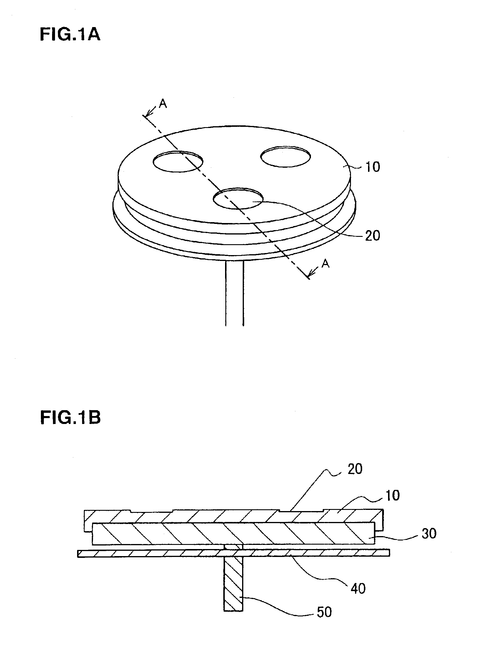
[0021]With regard to the first embodiment, a schematic perspective view inside a chamber of a vertical MOVPE crystal growth apparatus of high speed revolution type is illustrated as FIG. 1A. FIG. 1B is a sectional view showing typically on the line A—A of a MOVPE apparatus shown as FIG. 1A. Preferably, a material for a wafer carrier 10 to set a wafer is easy to be processed, capable of achieving a good thermal conduction and hard to be corroded with a material gas, such as carbon graphite and molybdenum. The wafer carrier 10, a jig for crystal growth, is placed on a susceptor 30 and heated on a heater 40 under the susceptor 30. The susceptor 30 supported by a rotation shaft 50 revolves so that the crystal growth may be uniform within the wafer carrier.

[0022]On the wafer carrier 10, a plurality of spot facing parts (hereinafter, referred to as a wafer pocket 20) to set the wafer horizontally are formed. Although FIG. 1 is illustrated so that three wafers can b...

Example

[0033](Second Embodiment)

[0034]In the second embodiment, a groove is formed on a spacer plate placed on the wafer pocket without making the grooving process directly on the wafer pocket as in the first embodiment. The spacer plate with the grooving process made thereon is mounted on the wafer pocket, on which the wafer is set. Preferably, a material for the spacer plate is high purity carbon and molybdenum, or a semiconductor wafer such as indium phosphide (InP), gallium arsenide (GaAs) and silicon (Si).

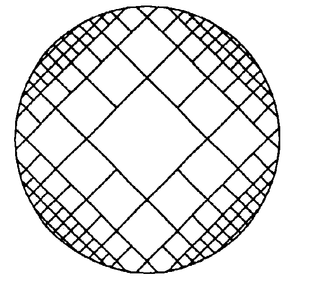
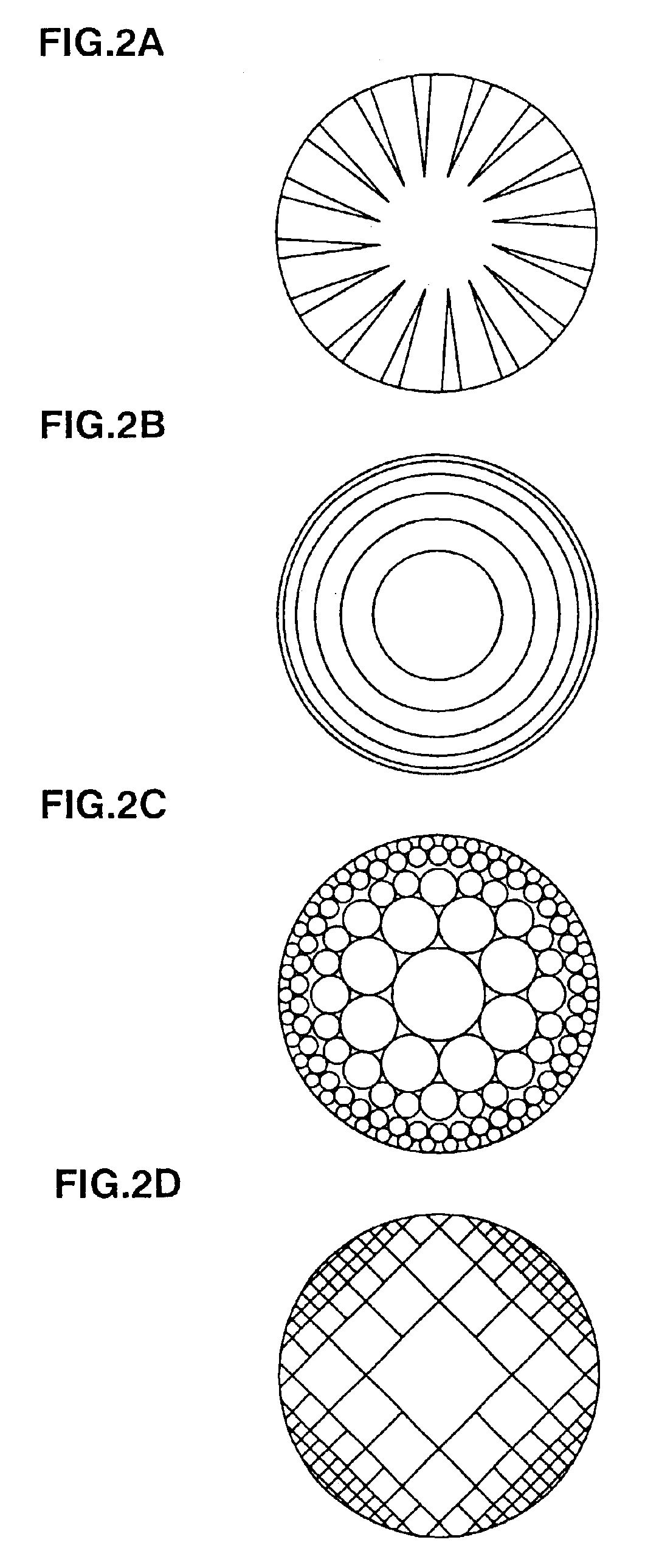
[0035]FIGS. 2A-D can be applied as a pattern diagram of groove on the spacer plate at this time. A plurality of grooves are formed on the spacer plate without making the grooving process on the wafer pocket. The depth of the plurality of grooves is deeper at the peripheral part of the spacer plate than at the central part thereof while the density of the plurality of grooves is higher at the peripheral part of the spacer plate than at the central part thereof. With regard to the groo...

Example

[0038](Third Embodiment)

[0039]In the first and second embodiments, a process is made on a jig in the MOVPE apparatus. In this third embodiment, on the other hand, a groove is formed directly on the rear surface of the wafer in order to make uniform the thermal conduction. The same pattern as the one shown in FIGS. 2A-D can be applied as the processing pattern of groove at this time. In the case of an element manufactured by using a normal crystal growth wafer, since a rear polishing is carried out in the final step of manufacturing the wafer to make the wafer thin-film, the element is not affected as a chip even if forming the groove on the rear surface.

[0040]A groove is formed having the pattern to uniform the thermal conduction, on the rear surface of the wafer before the crystal starts growing, by using a photolithography step and an etching step that are used generally in processing a surface of wafer conventionally. Patterning the groove by a photoresist by using a mask for pat...


PUM

PropertyMeasurementUnit
Temperatureaaaaaaaaaa
Diameteraaaaaaaaaa
Densityaaaaaaaaaa

Abstract

A method for manufacturing a semiconductor using a wafer carrier, wherein the temperature of a wafer can be made uniform with few differences in surface composition distribution. A plurality of grooves are formed at the bottom of a wafer pocket of a wafer carrier, to make uniform the temperature of the wafer surface by diffusing heat. The grooves are deeper at the peripheral part of the wafer than at the central part, and groove density is higher at the peripheral part than at the central part. The groove patterns may include a plurality of wedge-shaped grooves widening from the central part toward the peripheral part, a plurality of circular grooves with narrowing interval therebetween from the central part toward the peripheral part, circular grooves with the diameter shortened from the central part toward the peripheral part, and square grooves with shortened sides from the central part toward the peripheral part.

Description

BACKGROUND OF THE INVENTION[0001]1. Field of the Invention[0002]The present invention relates to a method for manufacturing a semiconductor by using a crystal growth apparatus in which a crystal growth is carried out by decomposing a source gas thermally on a wafer heated to reach a high temperature, especially by using a vertical MOVPE (Metal Organic Vapor Phase Epitaxy) apparatus of high speed revolution type.[0003]2. Description of the Related Art[0004]In the crystal growth using the MOVPE apparatus, the following document is disclosed as a method for improving an uniformity within a surface of a wafer of a growth layer: document “2001, International Conference on Indium Phosphide and Related Materials Post Deadline Papers pp.15-16. 13th IPRM 14-18, May 2001 Nara, Japan”.[0005]Recently, since an epitaxial wafer, which is a wafer with a thin film layer grown thereon, is used in most electronic devices, a mass production technology of the epitaxial wafer is indispensable. VPE (Vapo...

Claims


Application Information

Patent Timeline
IPC IPC(8): C30B25/10C23C16/458H01L21/205
CPCC30B25/10Y10S117/902
Inventor NAKAMURA, KOJI
Owner NEOPHOTONICS SEMICON GK
Why Eureka
Try Eureka