Semiconductor device

Active Publication Date: 2005-07-12
HITACHI LTD
View PDF8 Cites 39 Cited by
  • Summary
  • Abstract
  • Description
  • Claims
  • Application Information

AI Technical Summary

Benefits of technology

[0011]As described above, in order to avoid a requirement of using a high-energy ion implantation, this invention forms a trench in the surface of the substrate on the source side and provides a p-type gate region and a gate electrode in at least the bottom of the trench. This allows the channel width on the drain side to be narrowed even with a low energy ion implantatio

Problems solved by technology

Such a high energy ion implantation, however, requires a thick mask material for shielding, so that for a fine channel it is necessary to form a fine line with a large aspect ratio with a photolithography process, making the formation of fine channels more susceptible to process variations.
If we take process var

Method used


Image

  • Semiconductor device
  • Semiconductor device
  • Semiconductor device

Examples


Embodiment Construction

[0028]Now, embodiments of the present invention will be described in detail by referring to the accompanying drawings.

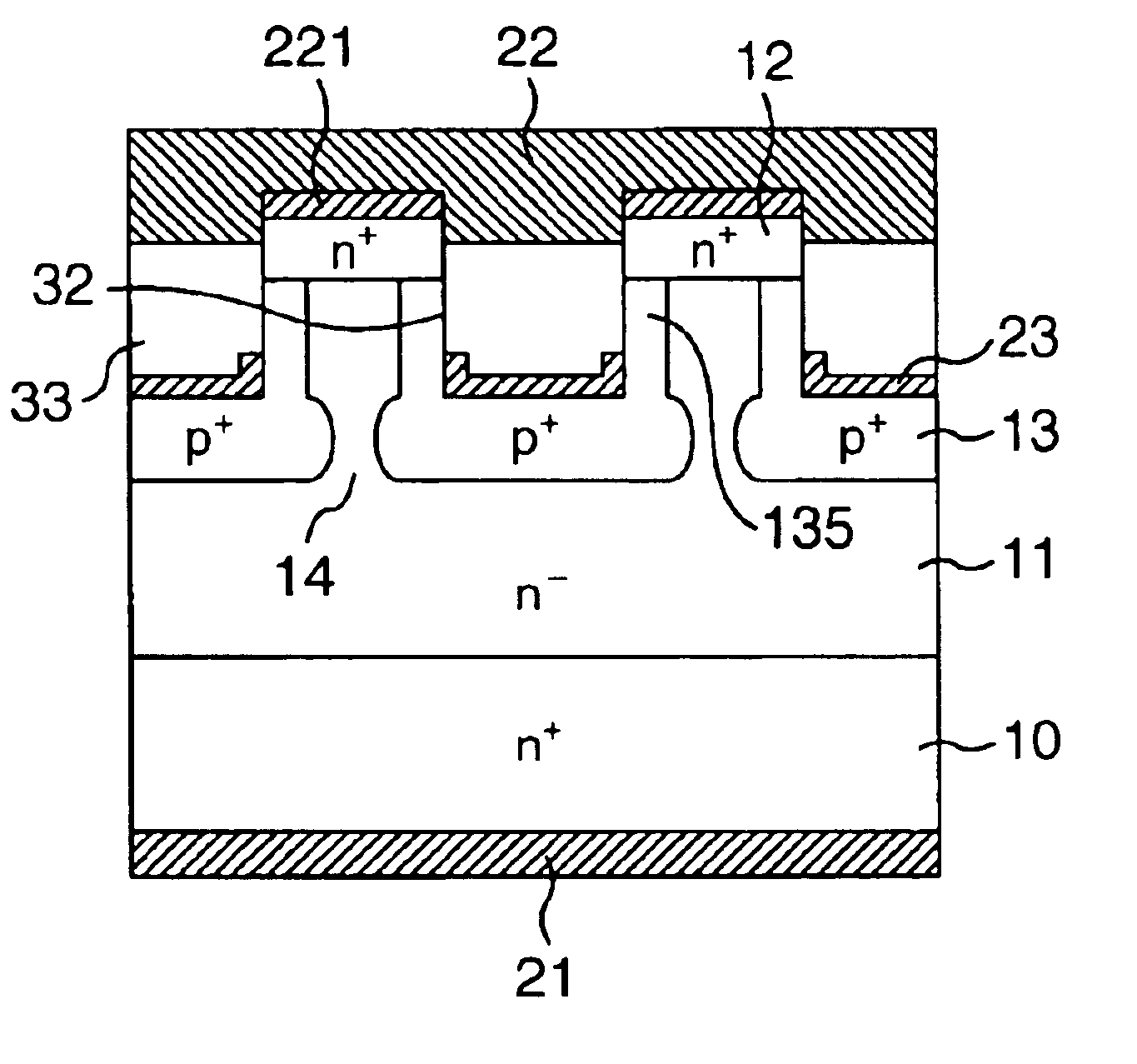
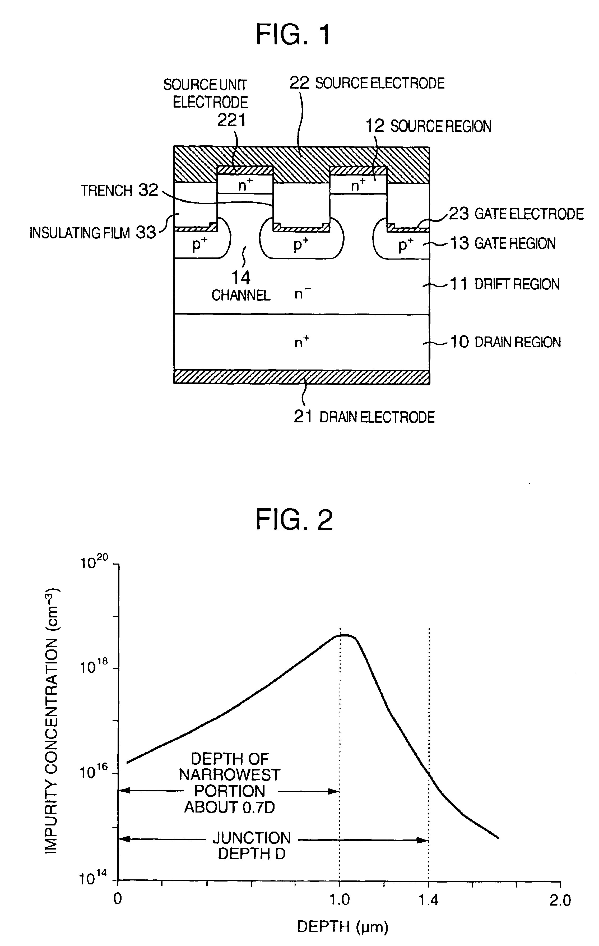
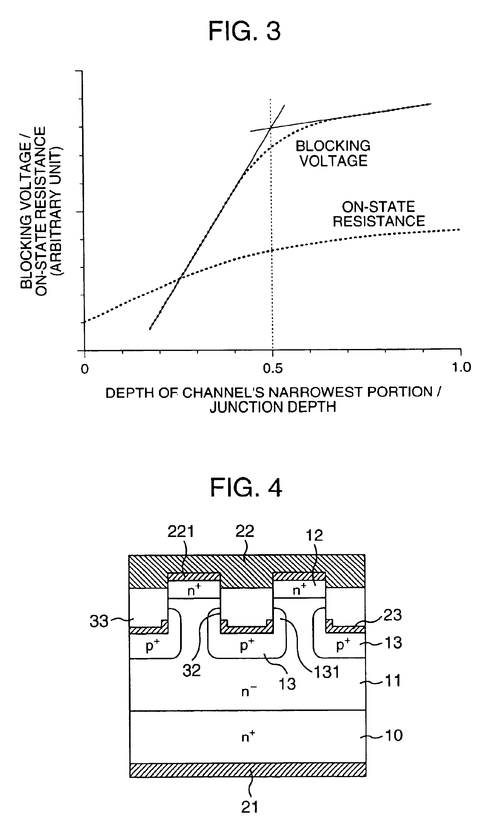
[0029]FIG. 1 is a cross-sectional view showing a structure of a SIT as a first embodiment of this invention. In the figure, numeral 11 denotes an n-type drift region, formed by a substrate of a first conductivity type with a low impurity concentration (which region will be referred to as either drift region 11 or substrate 11, hereinafter). An n+ drain region 10 is a first region formed on a first plane of the n-type drift region (substrate) 11 which has the same conductivity type n as, and a lower resistance than the drift region 11. An n-type source region 12 is a second region formed on a second plane of the substrate 11 which has the same conduction type n as the substrate 11. Reference number 32 designates a trench formed in the second plane of the drift region (substrate) 11. Spreading from a bottom of this trench 32 into the substrate 11 is a gate region 13, w...


PUM


Abstract

A semiconductor device includes a trench formed on a source side of a drift region, a p-type gate region and a gate formed at the bottom of the trench, and the source formed over the entire surface of the unit device through an insulating film. The narrowest portion of a channel of the device is deeper than one-half the junction depth of the p-type gate region. This allows the width of the channel on the drain side to be reduced even when a lower energy ion implantation manufacturing process is used.

Description

BACKGROUND OF THE INVENTION[0001]The present invention relates to improvements for transistors such as junction FETs (JFETs) and static induction transistors (SITs).[0002]Silicon carbide (SiC) has about 10 times as high a dielectric breakdown field as silicon (Si), so that a drift region provided to maintain a blocking voltage can be made thin and highly concentrated, thus reducing losses. Power semiconductor devices using SiC include junction FETs (JFETs) and static induction transistors (SITs).[0003]An example of an SIT that takes advantage of the features of SiC is described in JP-A-2001-94120. The structure in this Japanese patent has an n+ drain region, an n− drift region, an n+ source region, a p-type gate region and a p+ contact region. It also has a drain electrode, a source electrode and a gate electrode.[0004]SIT are transistors that turns an electric current on or off by a depletion layer expanding from the gate into a channel. By narrowing the channel width, which is equ...

Claims


Application Information

Patent Timeline
IPC IPC(8): H01L29/10H01L29/02H01L29/772H01L29/66H01L21/337H01L29/80H01L29/808
CPCH01L29/1066H01L29/7722H01L29/1608
Inventor ONOSE, HIDEKATSUHOMMA, HIDEOWATANABE, ATSUO
Owner HITACHI LTD
Why Eureka
Try Eureka