High-frequency module substrate device

a substrate device and high-frequency technology, applied in the direction of stacked capacitors, thin/thick film capacitors, instruments, etc., can solve the problems of reducing the characteristic of the substrate, reducing the parasitic capacity, and reducing the efficiency of the substrate, so as to achieve the effect of optimum impedance matching, reducing parasitic capacity, and improving characteristi

Inactive Publication Date: 2005-07-12
SONY CORP
View PDF7 Cites 25 Cited by
  • Summary
  • Abstract
  • Description
  • Claims
  • Application Information

AI Technical Summary

Benefits of technology

[0038]In the high frequency module substrate device according to the present invention, the coupler having frequency characteristic of λ/4 which has been caused to undergo distributed parameter design functions as a band-pass filter having pass-characteristic where carrier wave of, e.g., 5 GHz band is permitted to be passed. In the high frequency module substrate device, the thin film capacitor is connected to the coupler through the select switch means so that parallel capacity is loaded, whereby the coupler functions as a band-pass filter having pass-characteristic where carrier wave of frequency of, e.g., 2.45 GHz band is permitted to be passed. From this fact, the high frequency module substrate device can be compatibly used with respect to the wireless system where carrier wave of 2.45 GHz band is used and the wireless system where carrier wave of 5 GHz band is used. In the high frequency module substrate device, wavelength shortening effect by the base substrate of high dielectric constant and reduction of parasitic capacity are realized. As ...

Problems solved by technology

However, filters inserted between respective stages cannot be taken into IC.
Thus, this constitutes great obstacle in miniaturization and realization of light weight of communication terminal equipment.
In addition, since the high frequency transmitting/receiving circuit carries out amplification of one time at the high frequency stage, it becomes difficult to obtain sufficient gain.
Accordingly, there is the problem that the high frequency transmitting/receiving circuit requires cancel circuit for DC offset and additional low-pass filter, and the entire power consumption becomes large.
In both the superheterodyne system and the direct conversion system, as described above, the conventional high frequency transmitting/receiving circuits could not obtain sufficient characteristic with respect to the requirement specification such as miniaturization and/or lightweight, etc. of communication terminal equipment.
Such high frequency transmitting/receiving modules both have the problem that the step for forming the inductor portion is extremely complicated so that cost is increased by increase of the step.
On the other hand, in one chip high frequency transmitting/receiving module, electric interference of Si substrate intervening between high frequency circuit unit of analog circuit and base band circuit unit of digital circuit becomes great problem.
However, while the high frequency transmitting/receiving module functions when respective passive elements are formed within the layer where passive element is to be formed, there is the problem that Si substrate having conductivity constitutes obstacle to satisfactory high frequency characteristics of respective passive elements.
As a result, electric interference takes place between these respective wirings, and the problem of increase in cost due to the fact that wiring layer is formed so that it is caused to be of the multi-layer structure takes place.
Since the high frequency transmitting/receiving module is caused to be of package structure through the interposer substrate as described above, there is the problem that thickness or are...

Method used


Image

  • High-frequency module substrate device
  • High-frequency module substrate device
  • High-frequency module substrate device

Examples


Embodiment Construction

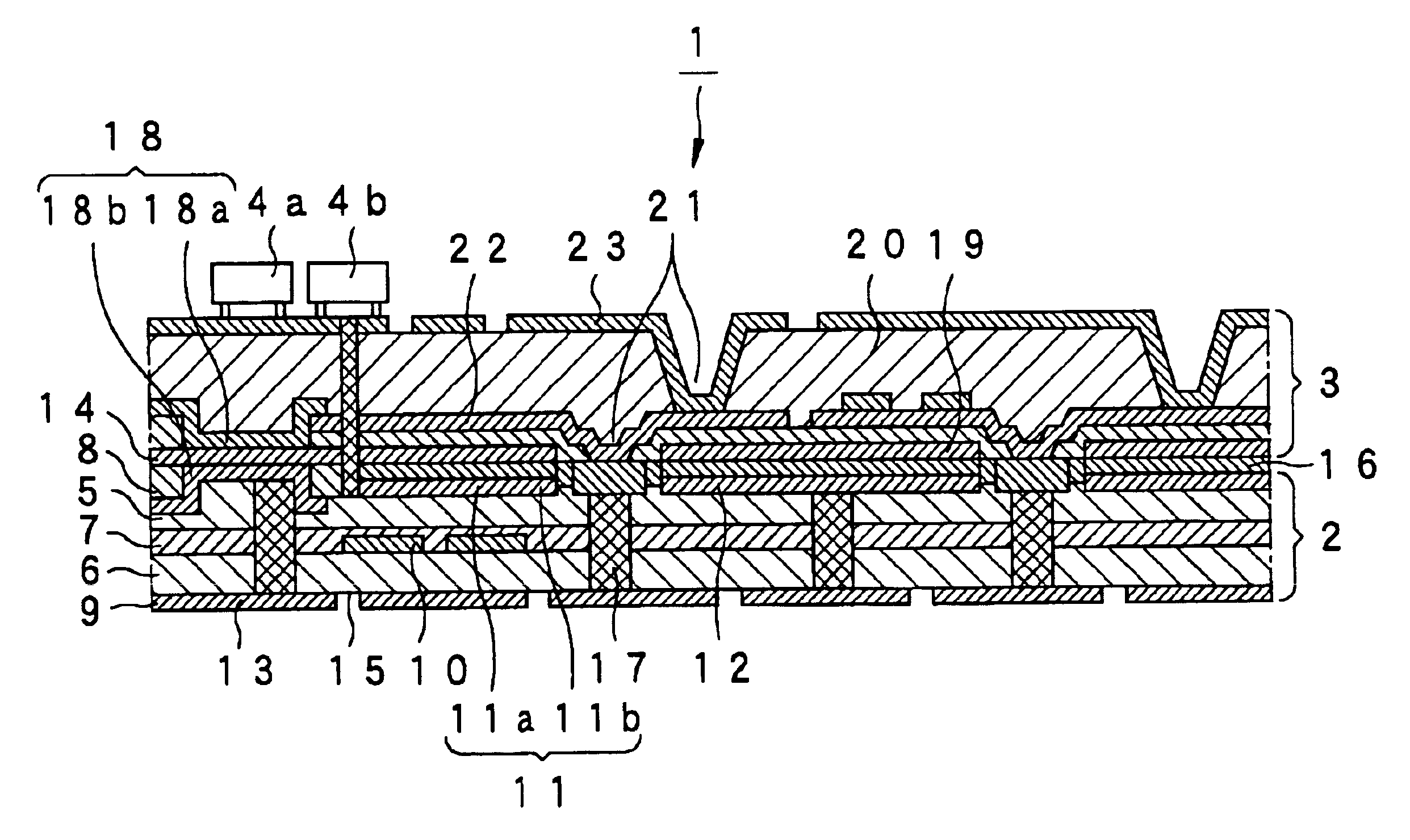
[0050]A high frequency module substrate device to which the present invention is applied will now be described in detail with reference to the attached drawings.

[0051]The high frequency module substrate device to which the present invention is applied (hereinafter abbreviated as high frequency module) is constituted as shown in FIG. 3, and constitutes a micro communication function module body having information communication function and / or storage function, etc. and mounted on various electronic equipments such as personal computer, mobile telephone or audio equipment, etc. or inserted into the above-described various equipments or withdrawn therefrom as an option.

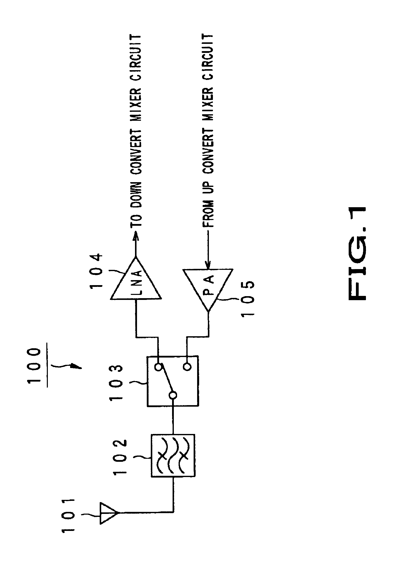
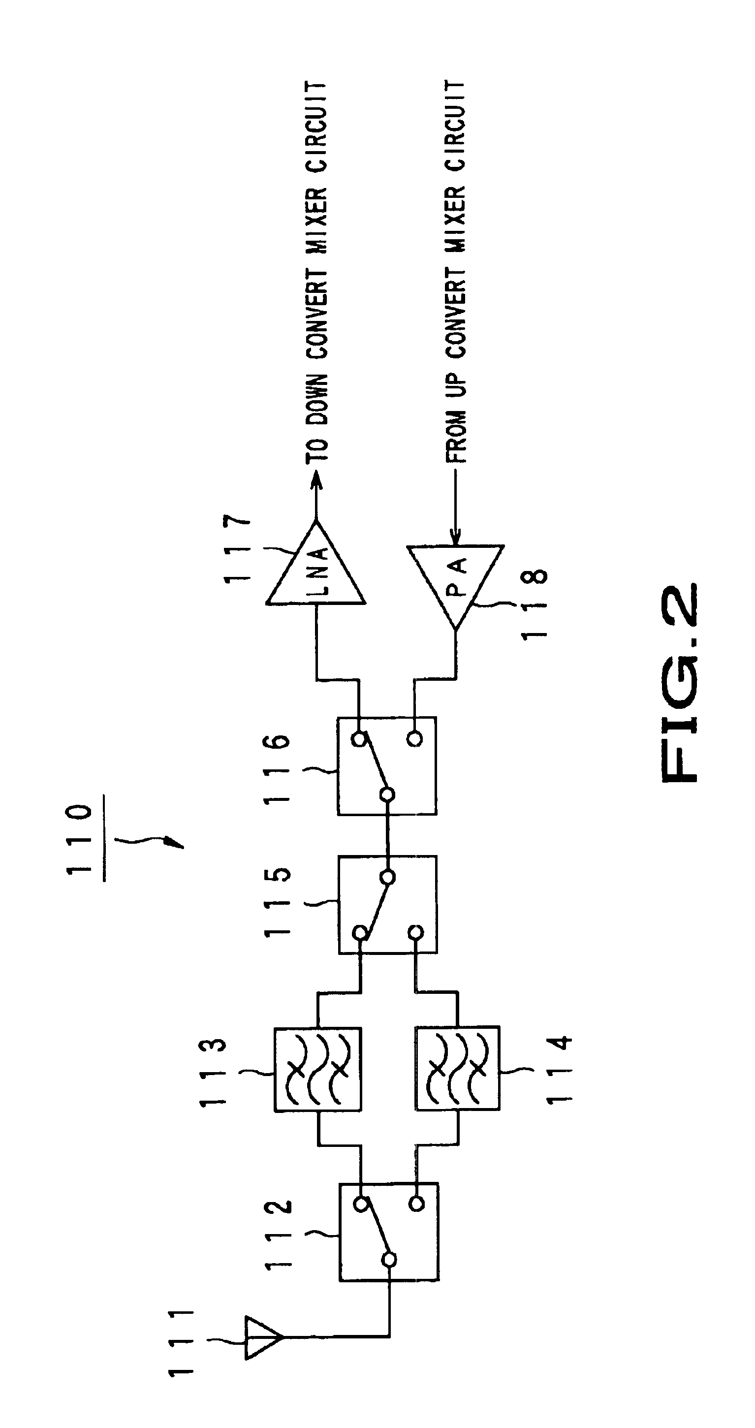
[0052]In the high frequency module 1 shown in FIG. 3 to which the present invention is applied, although the detail is omitted, there is formed a high frequency transmitting / receiving circuit unit by the superheterodyne system adapted for once carrying out conversion into intermediate frequency from transmit / receive sign...


PUM


Abstract

A high frequency module substrate device used in a high frequency module apparatus, which is adapted for switching pass-frequency characteristic of band-pass filter by switching and is adapted so that optimum band-pass filter characteristic is obtained in all pass-frequency bands, wherein a thin film capacitor element (18) is constituted between a base substrate (2) in which the uppermost layer is flattened with organic substrate being as core substrates (5), (6) to constitute a buildup formation surface (16) and a high frequency circuit unit (3) of lumped parameter design formed on the buildup formation surface in a laminated manner to carry out switching of load of parallel capacity with respect to a coupler (11) having frequency characteristic of λ/4 which has been caused to undergo distributed parameter design at the base substrate portion side of the thin film capacitor through switch means (4).

Description

BACKGROUND OF THE INVENTION[0001]The present invention relates to a high frequency module substrate device used in a high frequency module apparatus, and more particularly to a high frequency module substrate device used in a high frequency module apparatus constituting a micro-communication functional module mounted at various electronic equipments such as personal computer, mobile telephone, video equipment or audio equipment, etc. and having information communication function and / or storage function, etc.[0002]Various information such as music, voice (sound) or image, etc. have been handled with ease also by small sized information processing device such as personal computer or mobile computer, etc. with digitization of data. Band compression of such information is realized by voice Codec technology or image Codec technology, and environment in which such information are easily and efficiently delivered or distributed to various communication terminal equipments by digital commun...

Claims


Application Information

Patent Timeline
IPC IPC(8): H01P1/203H03H7/01H01P1/20H05K3/46H05K1/16H01P1/205H01P1/213H01G4/33H04B1/3822H04B1/40
CPCH01P1/20345H03H7/0123H05K1/162H05K3/4644H01P1/203
Inventor HIRABAYASHI, TAKAYUKI
Owner SONY CORP
Why Eureka
Try Eureka