Semiconductor substrate made of group III nitride, and process for manufacture thereof

a semiconductor and nitride technology, applied in the direction of crystal growth process, polycrystalline material growth, chemically reactive gas, etc., can solve the problems of inability to adapt to practical use, difficult bulk crystal growth of gan-based compound semiconductors, and inability to compensate, etc., to achieve low defect density, relieve strain, and high crystal quality

Inactive Publication Date: 2005-08-02
SUMITOMO CHEM CO LTD
View PDF11 Cites 115 Cited by
  • Summary
  • Abstract
  • Description
  • Claims
  • Application Information

AI Technical Summary

Benefits of technology

[0036]Since the present invention adopts a structure wherein a semiconductor layer of a group III nitrides are layered on the surface of a layer having voids, the present invention exerts the following effects:
[0037]Firstly, a semiconductor substrate of a group III nitride having a low defect density and a high crystal quality can be obtained. This is because the layer having voids acts as a strain-relieving layer, which will relieve strain caused by difference in lattice constants or coefficients of thermal expansion between the basal substrate and the second semiconductor layer of the group III nitride.
[0038]Secondly, the warp of the obtained semiconductor substrate can be reduced significantly, and thereby the yield in the photolithography step in the device process can be improved. This is because the layer having voids acts as a strain-relieving layer, which will relieve strain caused by difference in lattice constants or coefficients of thermal expansion between the basal substrate and the second semiconductor layer of the group III nitride.
[0039]Thirdly, since the basal substrate can be removed easily, a freestanding substrate of a well-shaped GaN single crystal without cracks and faults can be obtained easily. This is because a layer having voids are intervened between the basal substrate and the second semiconductor layer of a group III nitride, and thereby the basal substrate can be removed easily by means of a chemical agent, a mechanical impact or the like.
[0040]As a method for forming a GaN layer on a layer having voids, Japanese Patent Laid-Open No. 2000-277435 discloses a method wherein an anti-surfactant region (Si-remaining portion) is formed, and a GaN-based semiconductor is grown on this region while remaining a cavity to reduce dislocation density. In contrast, in the present invention, finer voids are formed densely and uniformly. By forming such voids, since the strain relieving effect becomes more significant, and the chemical agent becomes easier to permeate, it is easier to remove the basal substrate.
[0041]Although various methods may be selected for forming voids in a semiconductor layer of a group III nitride, the above-described method wherein the metal film is formed on the first semiconductor layer of the group III nitride, and then the substrate is heat-treated in an atmosphere containing hydrogen gas or a gas of a compound containing hydrogen can be preferably used. Furthermore, the substrate may be heat-treated in an atmosphere containing nitrogen gas, oxygen gas or a mixture thereof. By this heat treatment, the crystal structure of the first semiconductor layer of a group III nitride is decomposed, and component elements, such as nitrogen, will vaporize, resulting in the formation of voids in the layer. According to this method, a porous layer having a structure that can sufficiently relieve strain can be formed stably under good control. In particular, the adequate selection of heat-treatment conditions may attain a desired percentage of voids under good control.

Problems solved by technology

The bulk crystal growth of GaN-based compound semiconductors is difficult; therefore, a GaN substrate that could be adapted to practical use has not yet been obtained.
However, even this method cannot compensate the lattice-mismatch between the substrate and the crystal, and the GaN film has numerous defects.
These numerous defects are considered to interfere with the manufacture of a GaN-base LD.

Method used


Image

  • Semiconductor substrate made of group III nitride, and process for manufacture thereof
  • Semiconductor substrate made of group III nitride, and process for manufacture thereof
  • Semiconductor substrate made of group III nitride, and process for manufacture thereof

Examples


example 1

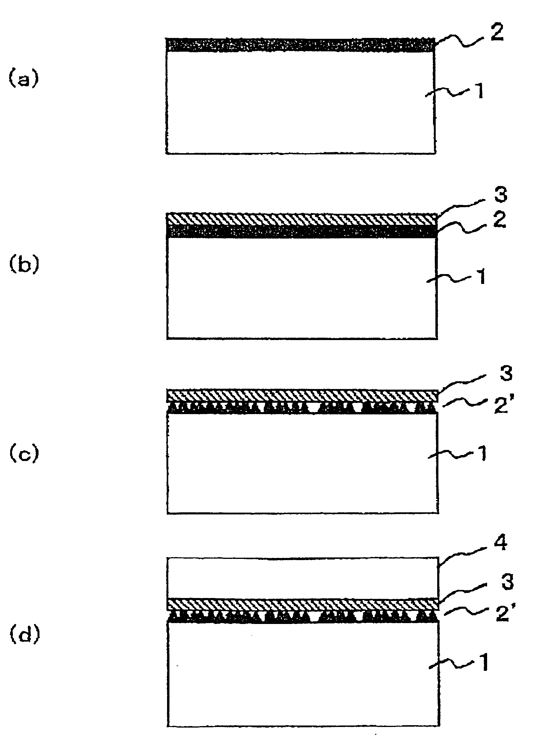
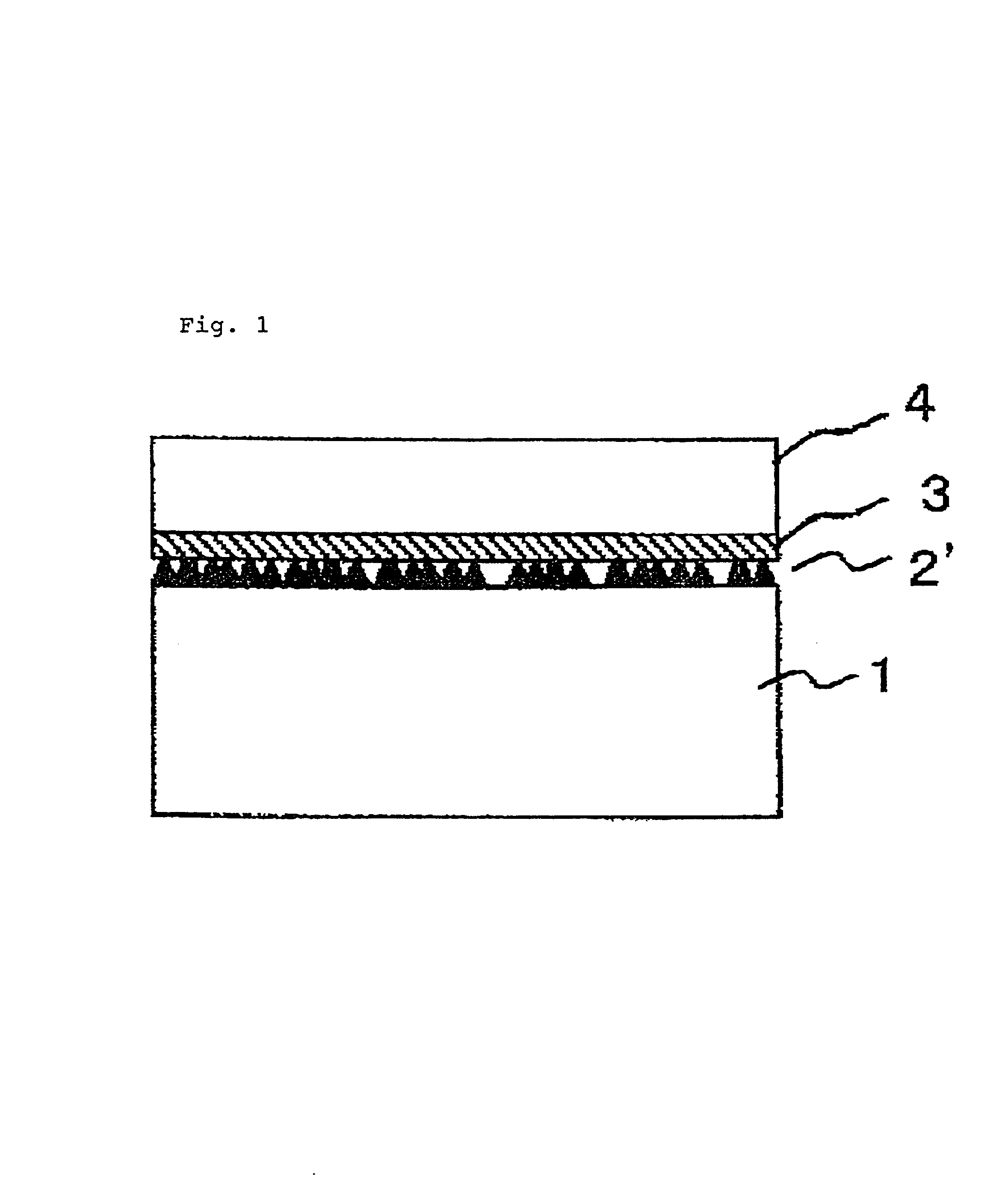
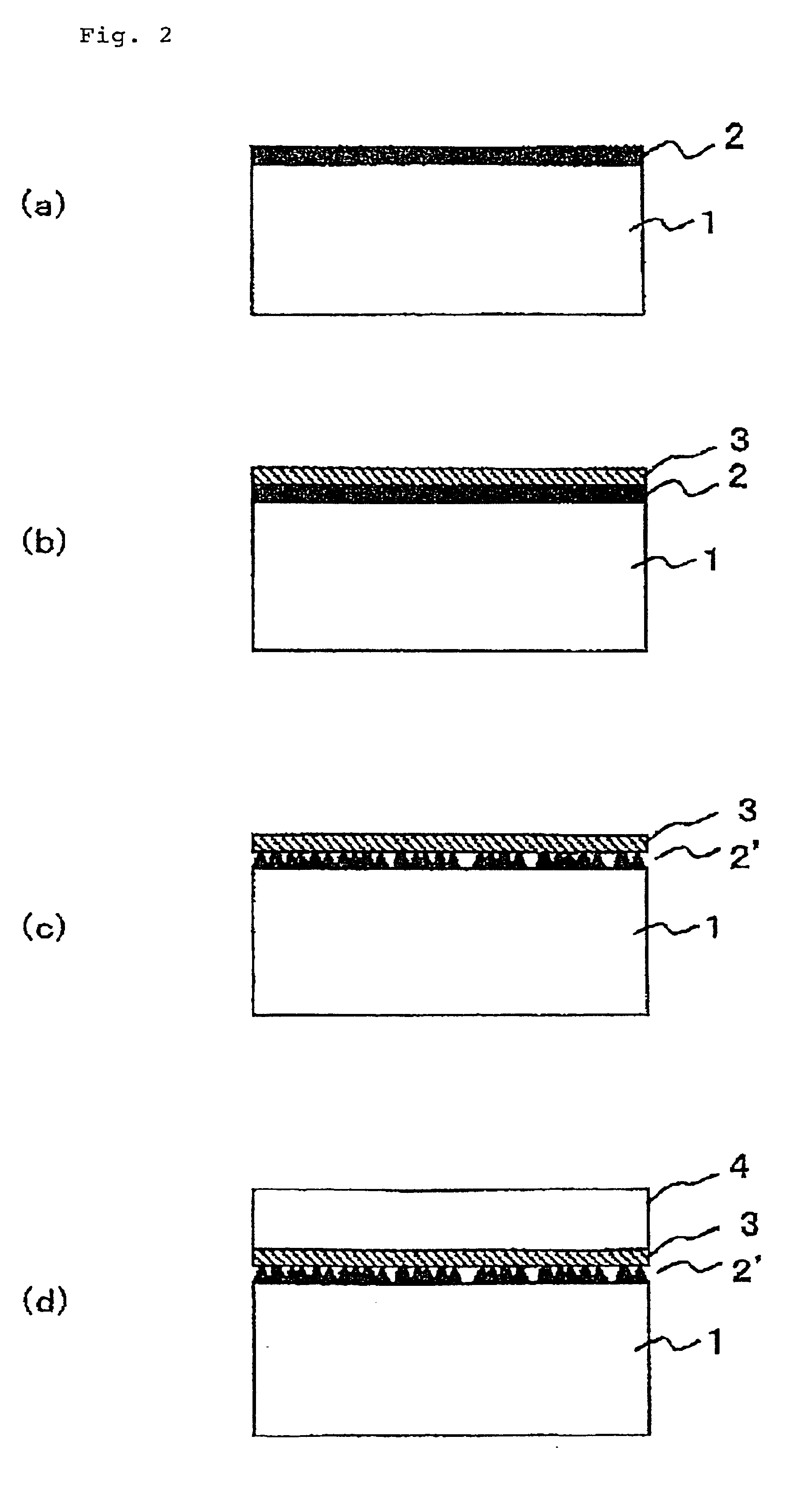
[0096]The structure of a semiconductor substrate obtained by the present invention is shown in FIG. 1, and sectional views of the process for manufacturing are shown in FIG. 2. The substrate was prepared by forming an undoped GaN layer 2 to a thickness of 400 nm on the C face ((0001) face) of a single-crystalline sapphire substrate 1 having a diameter of 2 inches, by means of MOCVD method with TMG (trimethyl gallium) and NH3 as starting materials (FIG. 2(a)). A titanium film 3 was vapor-deposited on the epitaxial GaN substrate to a thickness of 20 nm (FIG. 2(b)), and then loaded into the MOCVD chamber and the heat-treatment was carried out at 1050° C. for 20 minutes in the stream of Ar to which 20% H2 was mixed (FIG. 2(c)). Then, in the same chamber, 2 μm of a GaN layer 4 was grown using TMG and ammonia as starting materials on the titanium film 3 at 1050° C. (FIG. 2(d)). Thereby, a semiconductor substrate of a sectional structure as shown in FIG. 1 was obtained.

[0097]The surface of...

example 2

[0101]In order to confirm that the voids in the GaN layer 2′ was formed during the heat treatment of the substrate in Example 1, a substrate whereon titanium was vapor-deposited was heat-treated in the same method as in Example 1, and it was loaded out without growing the GaN layer thereon. Thereafter, the cross section was observed through an SEM. The result of SEM observation for the cross section of the substrate is shown in FIG. 7. It was confirmed from this result that voids same as those observed in Example 1 were formed in the GaN layer 2′ on the sapphire substrate.

example 3

[0102]The sectional views of the process of this example are shown in FIG. 2. The substrate was prepared by forming an undoped GaN layer 2 to a thickness of 200 nm on the C face of a single-crystalline sapphire substrate 1 having a diameter of 2 inches, by means of MOCVD method with TMG and NH3 as starting materials (FIG. 2(a)). A titanium film 3 was vapor-deposited on the epitaxial GaN substrate to a thickness of 25 nm (FIG. 2(b)), and then loaded into the MOCVD chamber and the heat-treatment was carried out at 1050° C. for 10 minutes in the stream of Ar to which 20% H2 was mixed (FIG. 2(c)), followed by further heat-treating it at 1050° C. for 30 minutes in the stream of N2. Then, in the same chamber, 2 μm of a GaN layer 4 was grown using TMG and ammonia as starting materials on the titanium film 3 at 1050° C. (FIG. 2(d)).

[0103]The surface of the epitaxial GaN substrate obtained thereby was very flat, and microscopic and SEM observations confirmed that its surface morphology was t...


PUM

PropertyMeasurementUnit
thicknessaaaaaaaaaa
thicknessaaaaaaaaaa
thicknessaaaaaaaaaa

Abstract

To provide a semiconductor substrate of a group III nitride with low defect density and little warp, this invention provides a process comprising such steps of:forming a GaN layer 2 on a sapphire substrate 1 of the C face ((0001) face); forming a titanium film 3 thereon; heat-treating the substrate in an atmosphere containing hydrogen gas or a gas of a compound containing hydrogen to form voids in the GaN layer 2; and thereafter forming a GaN layer 4 on the GaN layer 2′.

Description

FIELD OF THE INVENTION[0001]The present invention relates to a crystalline substrate of a nitride-based compound semiconductor, and a process for manufacture thereof.BACKGROUND TO THE INVENTION[0002]GaN-based compound semiconductors, such as gallium nitride (GaN), indium gallium nitride (InGaN) and gallium aluminum nitride (GaAlN), are spotlighted as materials for a blue-light-emitting diode (LED) and a laser diode (LD). Furthermore, development for the application of GaN-based compound semiconductors for electronic devices has been started utilizing their features of high heat resistance and environment friendliness.[0003]The bulk crystal growth of GaN-based compound semiconductors is difficult; therefore, a GaN substrate that could be adapted to practical use has not yet been obtained. A substrate for GaN growth widely put to practical use today is sapphire, and a method for the epitaxial growth of GaN on a single-crystal sapphire substrate by metal-organic vapor phase epitaxy (MO...

Claims


Application Information

Patent Timeline
Patent Type & Authority Patents(United States)
IPC IPC(8): C30B25/02H01L21/20H01L21/02H01L21/205
CPCC30B25/02C30B29/403C30B29/406H01L21/0242H01L21/02458H01L21/02491H01L21/02502H01L21/02513H01L21/0254H01L21/0262H01L21/02639H01L21/02647H01L21/20
Inventor USUI, AKIRASHIBATA, MASATOMOOSHIMA, YUICHI
Owner SUMITOMO CHEM CO LTD
Why Eureka
Try Eureka