Nitride semiconductor light-emitting device and optical apparatus including the same

a light-emitting device and nitride semiconductor technology, applied in semiconductor devices, semiconductor lasers, semiconductor lasers, etc., can solve the problem of hardly obtaining a light-emitting device having a high luminous efficiency, and achieve the effect of suppressing crystal phase separation, improving the crystallinity of the emission layer, and enhancing the luminous efficiency of the nitride semiconductor

Inactive Publication Date: 2005-08-02
SHARP KK
View PDF11 Cites 57 Cited by
  • Summary
  • Abstract
  • Description
  • Claims
  • Application Information

AI Technical Summary

Benefits of technology

[0005]A main object of the present invention is therefore to enhance the luminous efficiency in a nitride semiconductor light emitting device including an emission layer having a quantum well structure formed of nitride semiconductor by improving crystallinity of the emission layer and suppressing crystal phase separation.
[0007]In this way, the emission layer for causing effect of emitting light includes the quantum well layers and the barrier layers, and the quantum well layer has a smaller energy band gap as compared with the barrier layer.

Problems solved by technology

In the GaNAs / GaN emission layer described in Japanese Patent Laying-Open No. 10-270804, however, crystal phase separation of a hexagonal system having a high N concentration and a cubic system (zinc blende structure) having a low N concentration is liable to occur, and thus a light emitting device having a high luminous efficiency is hardly obtained.

Method used


Image

  • Nitride semiconductor light-emitting device and optical apparatus including the same
  • Nitride semiconductor light-emitting device and optical apparatus including the same
  • Nitride semiconductor light-emitting device and optical apparatus including the same

Examples


embodiment 1

[0028](Embodiment 1)

[0029]In the following, a nitride semiconductor laser diode device according to an embodiment 1 of the present invention will be described.

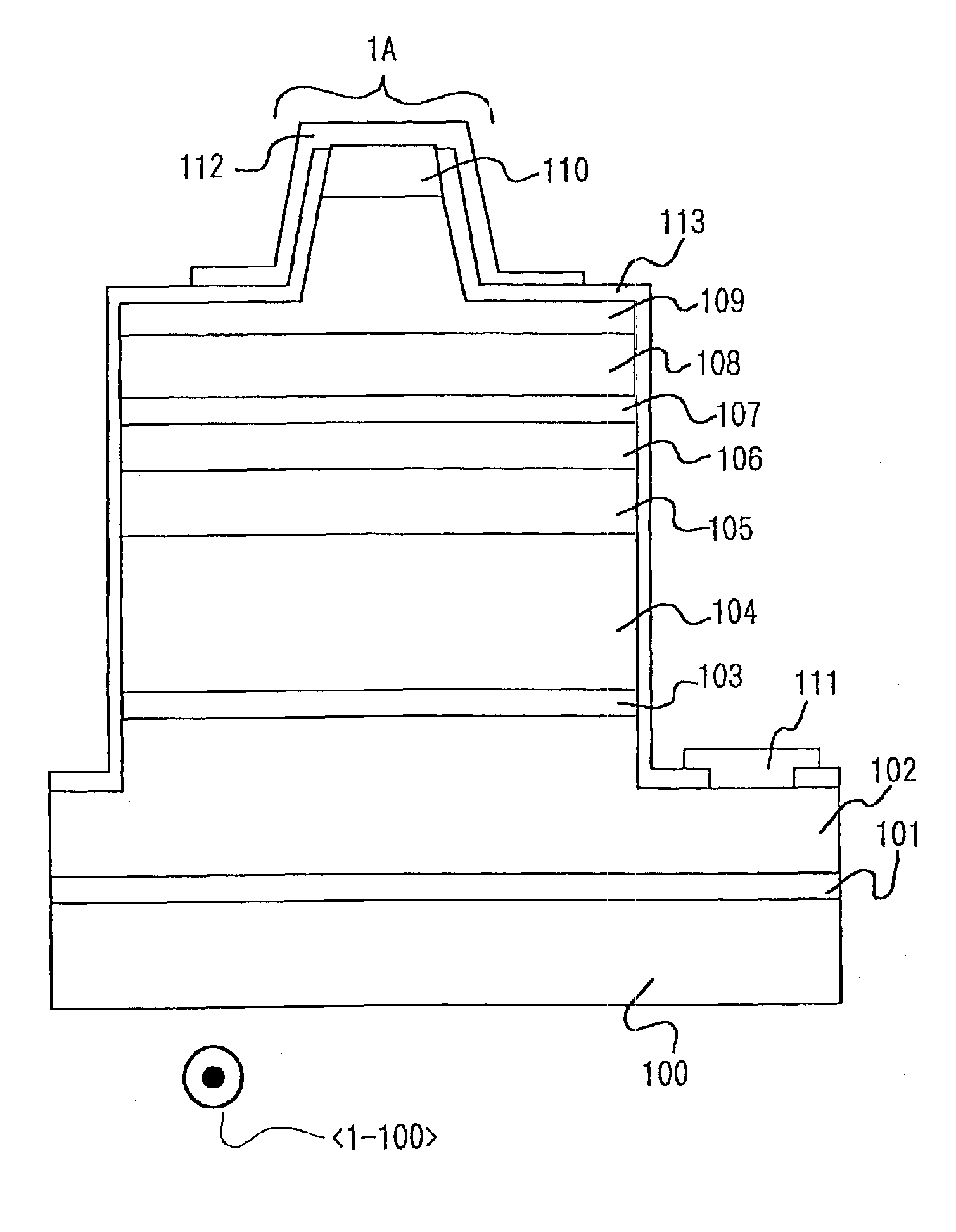
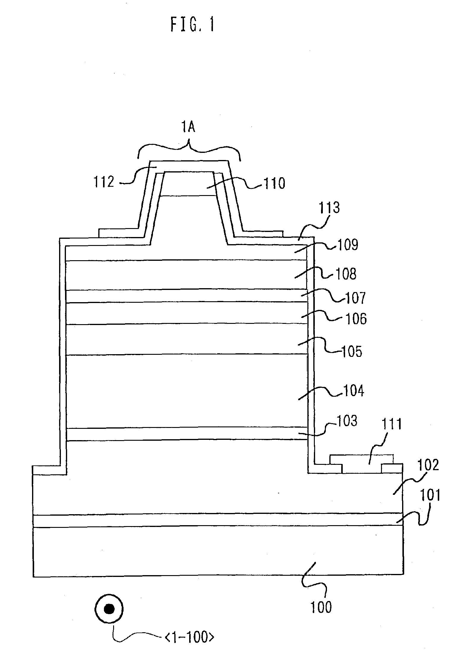
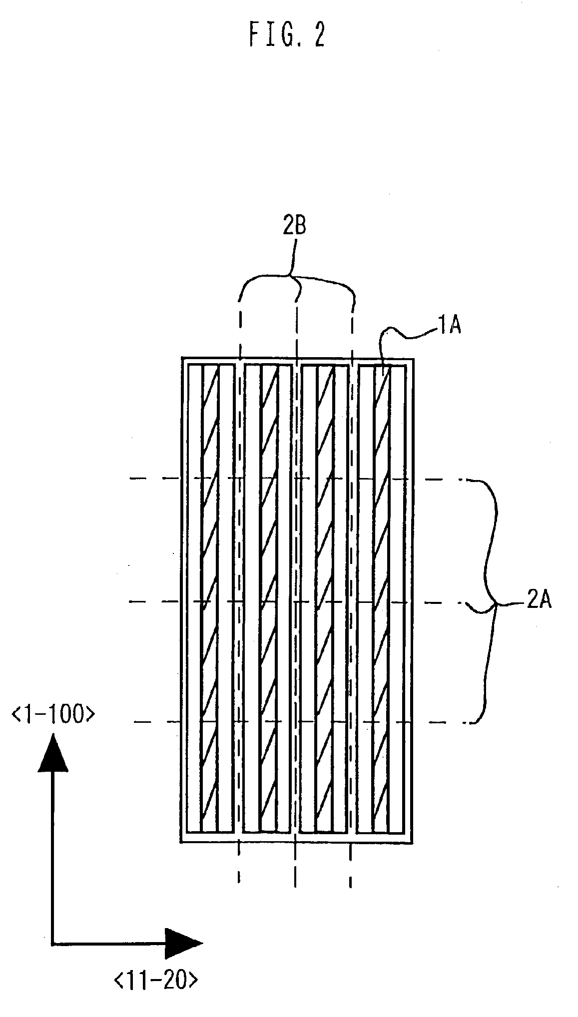
[0030]The nitride semiconductor laser diode device according to embodiment 1 shown in the schematic cross section of FIG. 1 includes a C-plane (0001) sapphire substrate 100, a GaN buffer layer 101, an n-type GaN contact layer 102, an n-type In0.07Ga0.93N anti-cracking layer 103, an n-type Al0.1Ga0.9N cladding layer 104, an n-type GaN light guide layer 105, an emission layer 106, a p-type Al0.2Ga0.8N blocking layer 107, a p-type GaN light guide layer 108, a p-type Al0.1Ga0.9 cladding layer 109, a p-type GaN contact layer 110, an n-type electrode 111, a p-type electrode 112 and an SiO2 dielectric film 113.

[0031]In fabrication of the laser diode device of FIG. 1, sapphire substrate 100 is first placed in an MOCVD apparatus, and GaN buffer layer 101 is grown to a thickness of 25 nm at a relatively low substrate temperature of 550°...

embodiment 2

[0074](Embodiment 2)

[0075]Embodiment 2 uses a variety of nitride semiconductor materials for the well layer and the barrier layer in the emission layer having a multiple quantum well structure as described in embodiment 1. The combinations of nitride semiconductor materials for the well layer and the barrier layer are shown in Table 3.

[0076]

TABLE 3barrier layerAlGaNAlGaNAsAlGaNPAlGaNSbInAlGaNInAlGaNAsInAlGaNPInAlGaNSbwell layerGaNAsΔ⊚⊚⊚⊚⊚⊚⊚GaNPΔ⊚⊚⊚⊚⊚⊚⊚GaNSbΔ⊚⊚⊚⊚⊚⊚⊚InGaNAsΔ⊚⊚⊚⊚⊚⊚⊚InGaNPΔ⊚⊚⊚⊚⊚⊚⊚InGaNSbΔ⊚⊚⊚⊚⊚⊚⊚AlGaNAsΔ⊚⊚⊚⊚⊚⊚⊚AlGaNPΔ⊚⊚⊚⊚⊚⊚⊚AlGaNSbΔ⊚⊚⊚⊚⊚⊚⊚InAlGaNAsΔ⊚⊚⊚⊚⊚⊚⊚InAlGaNPΔ⊚⊚⊚⊚⊚⊚⊚InAlGaNSbΔ⊚⊚⊚⊚⊚⊚⊚

[0077]In Table 3, Δ mark shows a less preferable combination of nitride semiconductor materials for the well layer and the barrier layer and ⊚ mark shows a preferable combination. It is noted that only an AlGaN barrier layer is less preferable in Table 3 for the reason as follows. Specifically, as described above, unless the growth temperature of the well layer of the present invention i...

embodiment 3

[0079](Embodiment 3)

[0080]In embodiment 3 shown in FIG. 6, n-type GaN substrate 700 having a C-plane ({0001}plane) as a main surface was used in place of sapphire substrate 100 used in embodiment 1. When the GaN substrate is used, GaN buffer layer 101 may be omitted and n-type GaN layer 102 maybe grown directly on the GaN substrate. Since the GaN substrate commercially available at present does not have good enough crystallinity and surface morphology, however, GaN buffer layer 101 is preferably inserted in order to improve these.

[0081]Since n-type GaN substrate 700 is used in embodiment 3, n-type electrode 111 can be formed on the rear surface of GaN substrate 700. Furthermore, since the GaN substrate can have a very flat cleavage end surface, a Fabry-Pérot resonator having a resonator length of 300 μm can be fabricated with a small mirror loss. It is noted that similarly to embodiment 1 the resonator length is preferably within a range from 300 μm to 1000 μm in general. The mirror...


PUM


Abstract

A nitride semiconductor light emitting device includes an emission layer (106) having a multiple quantum well structure where a plurality of quantum well layers and a plurality of barrier layers are alternately stacked. The quantum well layer is formed of XN1-x-y-zAsxPySbz (0≦x≦0.15, 0≦y≦0.2, 0≦z≦0.05, x+y+z>0) where X represents one or more kinds of group III elements. The barrier layer is formed of a nitride semiconductor layer containing at least Al.

Description

CROSS-REFERENCE TO RELATED APPLICATIONS[0001]This application is a National Phase under 35 U.S.C. § 371 of International Application No. PCT / JP01 / 03825 filed on May 7, 2001 which claims priority to Japanese Patent Application No. 2000-158189 filed on May 29, 2000, the contents of each of which are incorporated herein by reference in their entirety.TECHNICAL FIELD[0002]The present invention relates to a nitride semiconductor light emitting device with high luminous efficiency and an optical apparatus using the same.BACKGROUND ART[0003]Conventionally, nitride semiconductor has been used or studied for a light emitting device or a high power semiconductor device. In the case of a nitride semiconductor light emitting device, a light emitting device in a wide color range from blue to orange can be fabricated. Recently, by utilizing the characteristics of the nitride semiconductor light emitting device, a blue or green light emitting diode or a bluish violet semiconductor laser has been d...

Claims


Application Information

Patent Timeline
Patent Type & Authority Patents(United States)
IPC IPC(8): H01S5/343H01L33/00H01S5/00H01S5/30H01S5/20H01L33/06H01L33/32H01L33/34H01S5/323
CPCB82Y20/00H01L33/06H01L33/32H01S5/00H01S5/34333H01S5/2009H01S5/305H01S5/3434H01S5/34346
Inventor TSUDA, YUHZOHYUASA, TAKAYUKIITO, SHIGETOSHI
Owner SHARP KK
Why Eureka
Try Eureka