DC-DC converter implemented in a land grid array package

a technology of dc-dc converter and land grid array, which is applied in the direction of electric variable regulation, process and machine control, instruments, etc., can solve the problems of reducing the effectiveness of the package in terms of size reduction, component density and most importantly power density, and the product is packaged in a micro lead frame (mlf) that does not readily accommodate a large number of discrete passive components, so as to improve the thermal dissipation characteristics of the package and reduce the cost of the a land grid array package and dc-dc-dc-dc-dc-dc-dc-dc-dc-dc-dc-dc-dc-dc-dc-dc-dc-dc-dc-dc-dc-dc-dc-dc-dc-dc-dc-dc-dc-dc-dc-dc-dc-dc-dc-dc-dc-dc-dc-dc-dc-dc-dc-dc-dc-dc-dc-d

Inactive Publication Date: 2005-09-06
PWER BRIDGE
View PDF7 Cites 64 Cited by
  • Summary
  • Abstract
  • Description
  • Claims
  • Application Information

AI Technical Summary

Benefits of technology

[0016]Another aspect of the present invention is to increase the thermal dissipation characteristics of the package. In one embodiment, a high density via array is electrically and thermally coupled to each semiconductor die. The high density via array optimizes the total number of vias that may be positioned under the semiconductor die (within the physical outline of the power semiconductor die). Each high density via array dissipates the heat generated by the semiconductor die more efficiently than conventional via arrays.

Problems solved by technology

Electronic systems face significant challenges for further size reductions, component density and most importantly power density.
Often, the product is packaged in a micro lead frame (MLF) that does not readily accommodate a large number of discrete passive components.
Consequently, the discrete passive components must be located externally—reducing the effectiveness of the package in terms of size reduction.
For example, circuits such as the boost circuit and compensation components are frequently located to the exterior of the product and consume additional board space.
These separately housed components occupy a significant amount of space on a printed circuit board (PCB).
These components require careful layout and trace routing to avoid stray inductances that can result in poor performance, or in some cases, device failure.

Method used


Image

  • DC-DC converter implemented in a land grid array package
  • DC-DC converter implemented in a land grid array package
  • DC-DC converter implemented in a land grid array package

Examples


Embodiment Construction

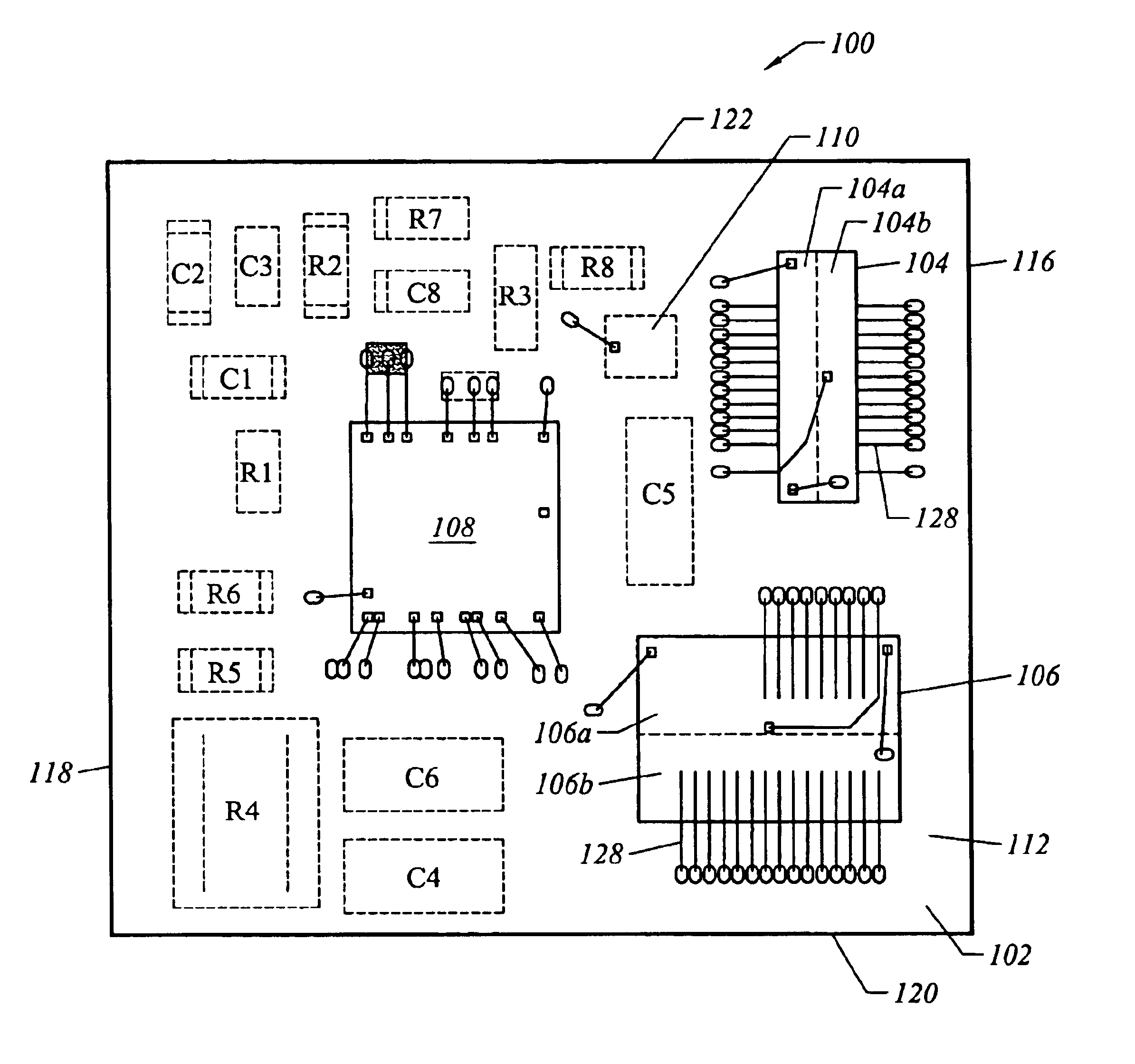
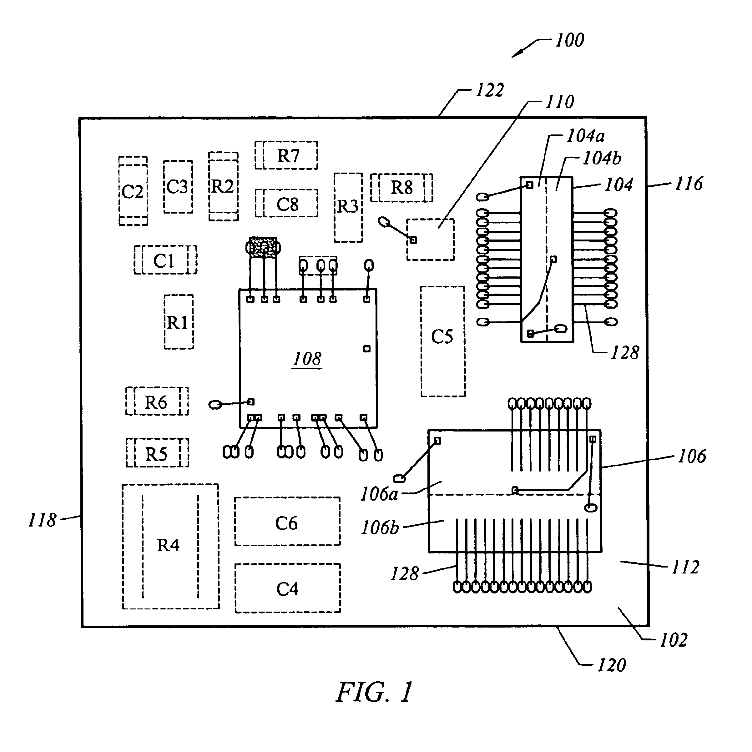
[0026]In general, the present invention integrates a DC—DC converter into an LGA package in order to meet the demanding electrical and thermal requirements for a board-level distributed power architecture in a minimum footprint. More particularly, the present invention provides a highly-efficient point-of-load DC—DC power converter adapted to deliver low voltages at high currents in close proximity to loads. The LGA package integrates all required active components of the DC—DC power converter, including a synchronous buck PWM controller, driver circuits, and MOSFET devices.

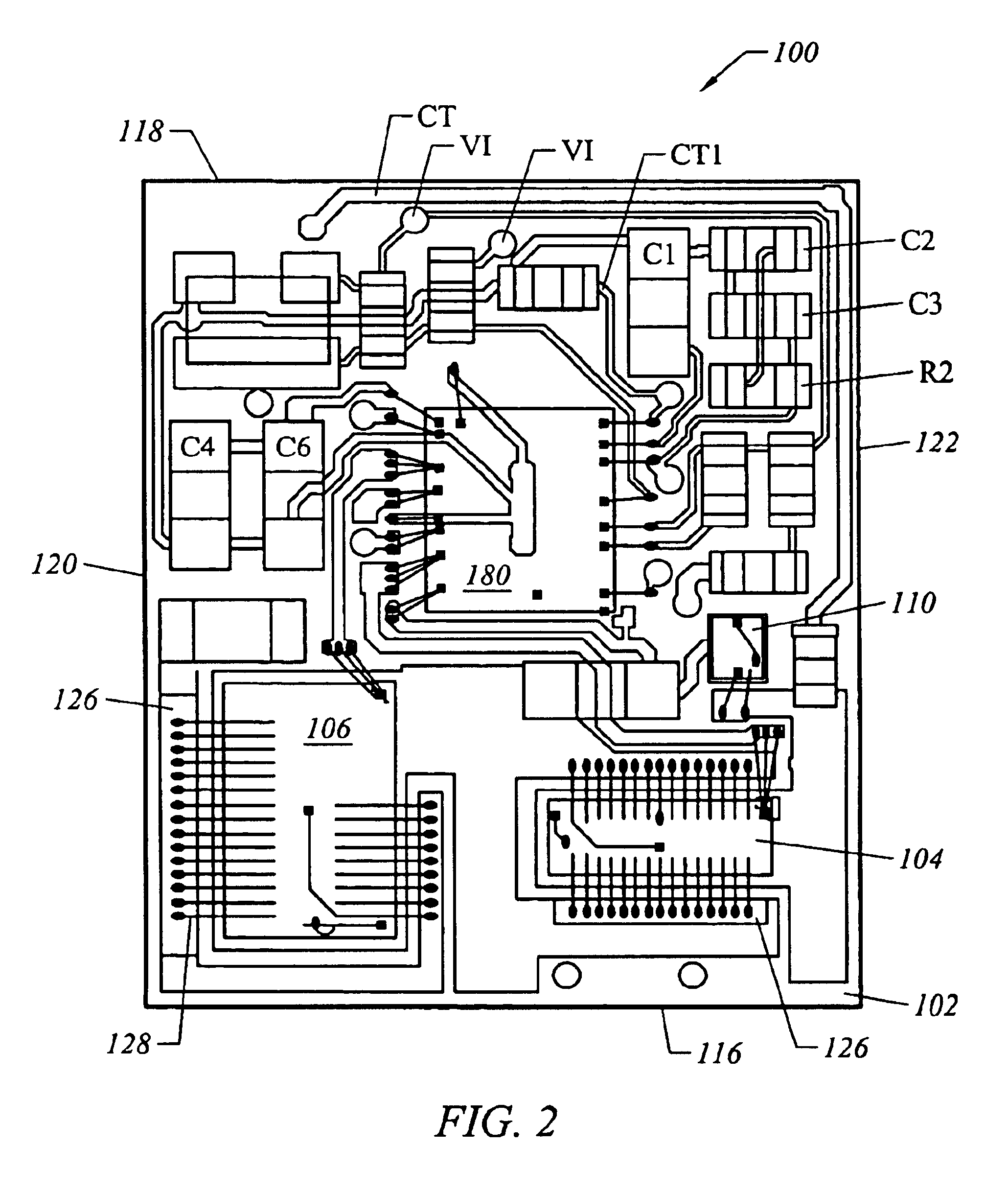
[0027]FIGS. 1-2 illustrate a top view of a power semiconductor package 100 according to one aspect of the present invention. The power semiconductor package 100 includes, among other components that will be discussed later, a substrate 102, a first power semiconductor die 104, a second power semiconductor die 106, a third semiconductor die 108, a fourth semiconductor die 110, and a plurality of discrete passive c...


PUM


Abstract

A semiconductor chip package that includes a DC—DC converter implemented with a land grid array (LGA) package for interconnection and surface mounting to a printed circuit board. The LGA package integrates all required active components of the DC—DC power converter, including a synchronous buck PWM controller, driver circuits, and MOSFET devices. In particular, the LGA package comprises a substrate having a top surface and a bottom surface, with a DC—DC converter provided on the substrate. The DC—DC converter including at least one power silicon die disposed on the top surface of the substrate. A plurality of electrically and thermally conductive pads are provided on the bottom surface of the substrate in electrical communication with the DC—DC converter through respective conductive vias. The plurality of pads include first pads having a first surface area and second pads having a second surface area, the second surface area being substantially larger than the first surface area. Heat generated by the DC—DC converter is conducted out of the LGA package through the plurality of pads.

Description

RELATED APPLICATION DATA[0001]This is a continuation-in-part of copending application Ser. No. 10 / 423,603, filed Apr. 24, 2003, for DC—DC CONVERTER IMPLEMENTED IN A LAND GRID ARRAY PACKAGE.BACKGROUND OF THE INVENTION[0002]1. Field of the Invention[0003]The present invention relates generally to a power supply implemented with microelectronic components. More specifically, an embodiment of the present invention integrates a high-current buck regulator into a land grid array (LGA) package in order to meet the demanding electrical and thermal requirements for a board-level distributed power architecture in a minimum footprint.[0004]2. Description of Related Art[0005]Electronic systems face significant challenges for further size reductions, component density and most importantly power density. Many obstacles need to be overcome to meet up to these challenges. Effective heat dissipation and its management coupled with low resistance and low inductance interconnect, combined with the nee...

Claims


Application Information

Patent Timeline
Patent Type & Authority Patents(United States)
IPC IPC(8): H01L23/34H01L23/367H01L23/48H01L23/36H01L23/538H01L25/16H02M3/00H02M3/10H02M3/158
CPCH01L23/36H01L23/3677H01L23/5386H01L25/165H02M3/00H02M3/1588H01L2224/48227H01L2224/48471H01L2224/49111H01L2924/01077H01L2924/01078H01L2924/13091H01L2924/14H01L2924/19041H01L2924/30107H01L2924/3011H02M3/10Y02B70/1466H01L24/48H01L24/49H01L2924/00H01L2224/45147H01L2224/32225H01L2924/10253H01L2924/01015H01L2924/00014H01L24/45H01L2224/05554H01L2924/19105H01L2924/00011Y02B70/10H02M3/003H01L2224/45099H01L2224/05599H01L2924/01033H01L27/00H01L25/00H01L23/02
Inventor DIVAKAR, MYSORE PURUSHOTHAMKEATING, DAVIDRUSSELL, ANTOIN
Owner PWER BRIDGE
Why Eureka
Try Eureka