
Use of dilute steam ambient for improvement of flash devices

a technology of flash devices and ambient, which is applied in the direction of semiconductor devices, electrical apparatus, transistors, etc., can solve the problems of finite soft error rate and affecting the performance of underlying devices, and achieve uniform thickness, improve the performance of the resulting device structure, and increase the oxide thickness of a storage dielectric layer at the same time

Inactive Publication Date: 2005-09-27
MICRON TECH INC
View PDF17 Cites 10 Cited by
  • Summary
  • Abstract
  • Description
  • Claims
  • Application Information

AI Technical Summary

Benefits of technology

[0009]In accordance with one aspect of the present invention, a method is provided for fabricating an integrated circuit. The method includes providing a silicon semiconductor substrate and forming a stacked gate structure comprising an oxide-silicon interface defined by an initial oxide layer directly in contact with a silicon layer. Upon patterning the stacked gate structure to define a gate stack that includes the oxide-silicon interface, a final oxide layer is formed with additional silicon oxide bonds in the region of the oxide-silicon interface. This result is achieved by exposing the patterned gate stack to elevated temperatures and a dilute steam ambient.
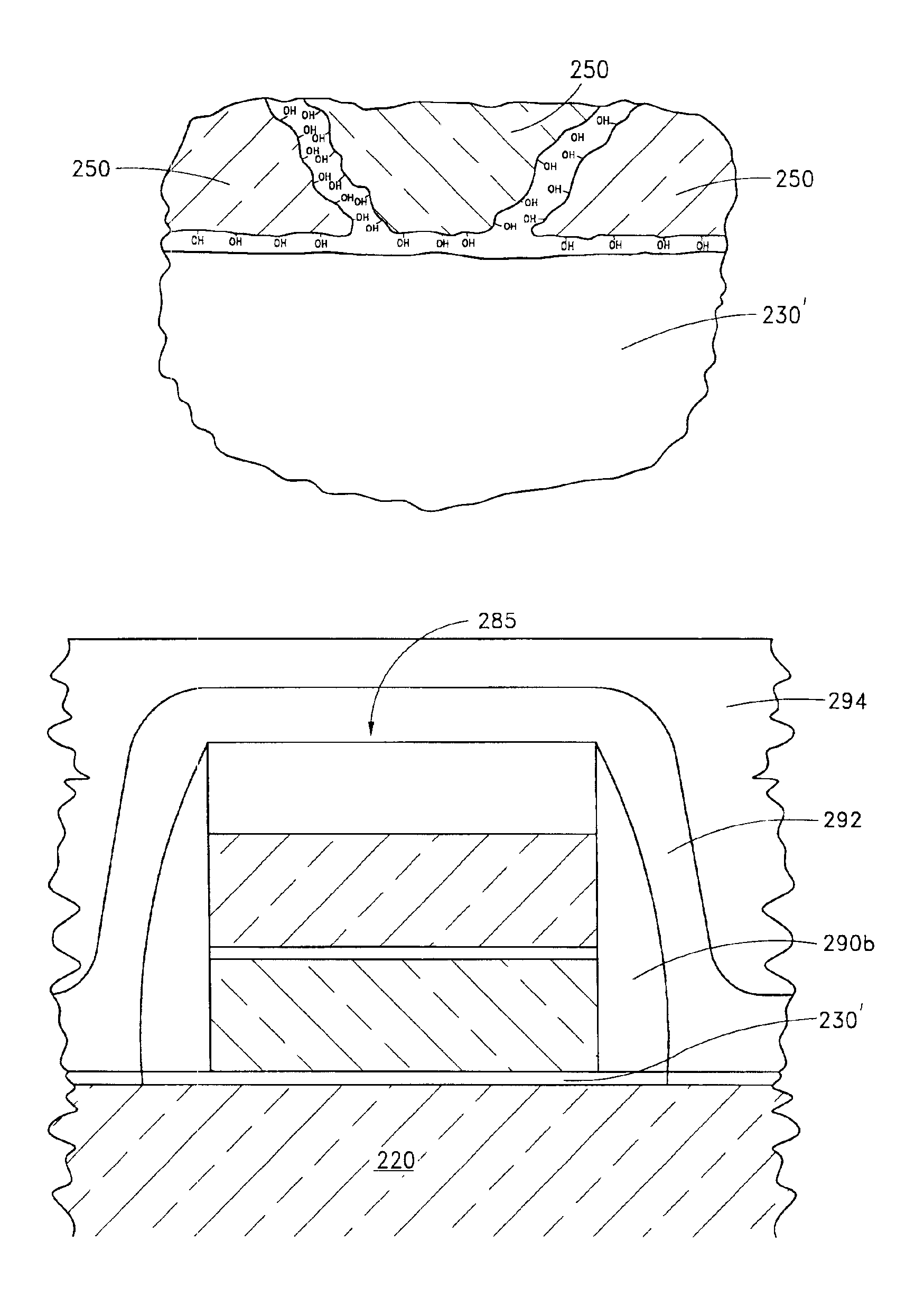
[0013]In the illustrated embodiments, a stacked gate structure is formed on the surface of a silicon semiconductor substrate, wherein the stacked gate structure comprises an initial tunnel dielectric layer, one or more polysilicon layers, and an initial storage dielectric layer comprising one or more initial oxide layers. After patterning, the stacked gate structure is exposed to elevated temperatures and a dilute steam ambient comprising steam and hydrogen. This dilute steam ambient process yields OH radicals which readily diffuse through the initial oxide and form additional oxide material substantially uniformly along the oxide-silicon interfaces of the stacked gate structure. The oxidation rate is controlled by diluting the steam with carrier and preferably hydrogen-bearing gas, and by keeping the oxidation temperature moderate. As a result, oxidation is slower relative to the lateral diffusion of OH species from the gate sidewalls across the entire interface. The final tunnel dielectric layer thus has a substantially uniform thickness. Most preferably, the oxide thickness of a storage dielectric layer is simultaneously increased.
[0014]Advantageously, the exposure of the stacked gate structure to the dilute steam ambient improves the performance of the resulting device structures. First, the number of defects, such as oxygen vacancies and dangling bonds, in the region of the final tunnel dielectric layer is reduced by the additional oxide material. Second, consumption of thermal budget can be dramatically reduced due to the relatively low temperatures and time of the dilute steam ambient oxidation in forming a substantial fraction of the final storage dielectric layer. And third, the grain boundaries of polysilicon layers within the stacked gate structure are passivated during the dilute steam oxidation, thereby reducing the effect of the grain boundaries on the erase characteristics of the resulting devices.

Problems solved by technology

Such out-diffusion might otherwise affect the performance of underlying devices.
While processes have been developed to improve gate dielectric quality, as measured by improved data retention in flash memory devices, for example, a finite soft error rate remains.

Method used


Image

  • Use of dilute steam ambient for improvement of flash devices
  • Use of dilute steam ambient for improvement of flash devices
  • Use of dilute steam ambient for improvement of flash devices

Examples


Embodiment Construction

[0027]While illustrated in the context of an electrically erasable programmable read only memory (EEPROM) device for flash memory circuits, persons skilled in the art will readily find application for the present invention to fabrication of other semiconductor integrated circuit devices. In particular, methods disclosed herein are applicable to improving dielectric-conductor interfaces in a wide variety of device designs with a wide variety of process flows. The methods described herein, however, have particular utility for improving the performance of dielectric layers in flash memory gate stacks.

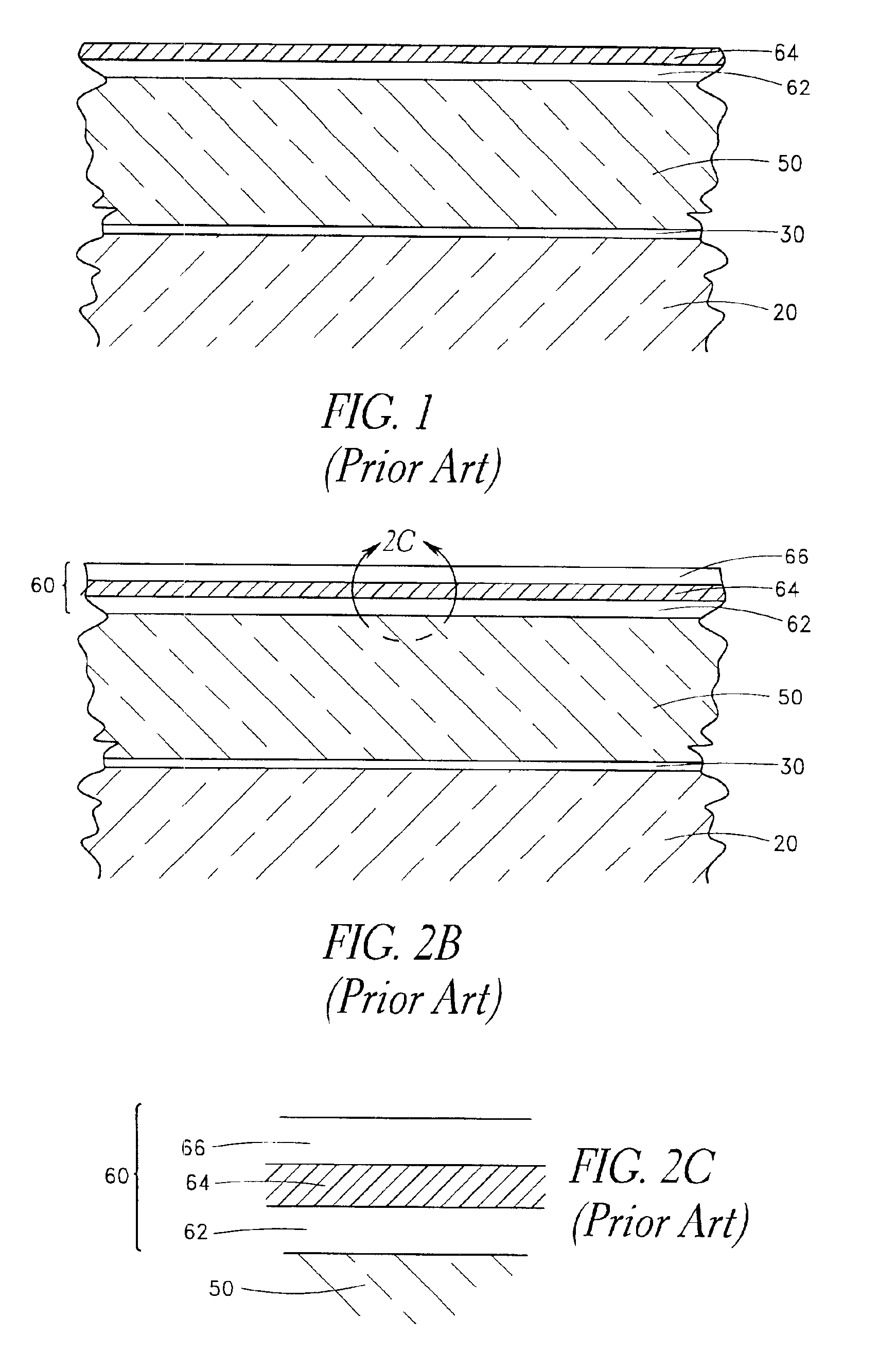
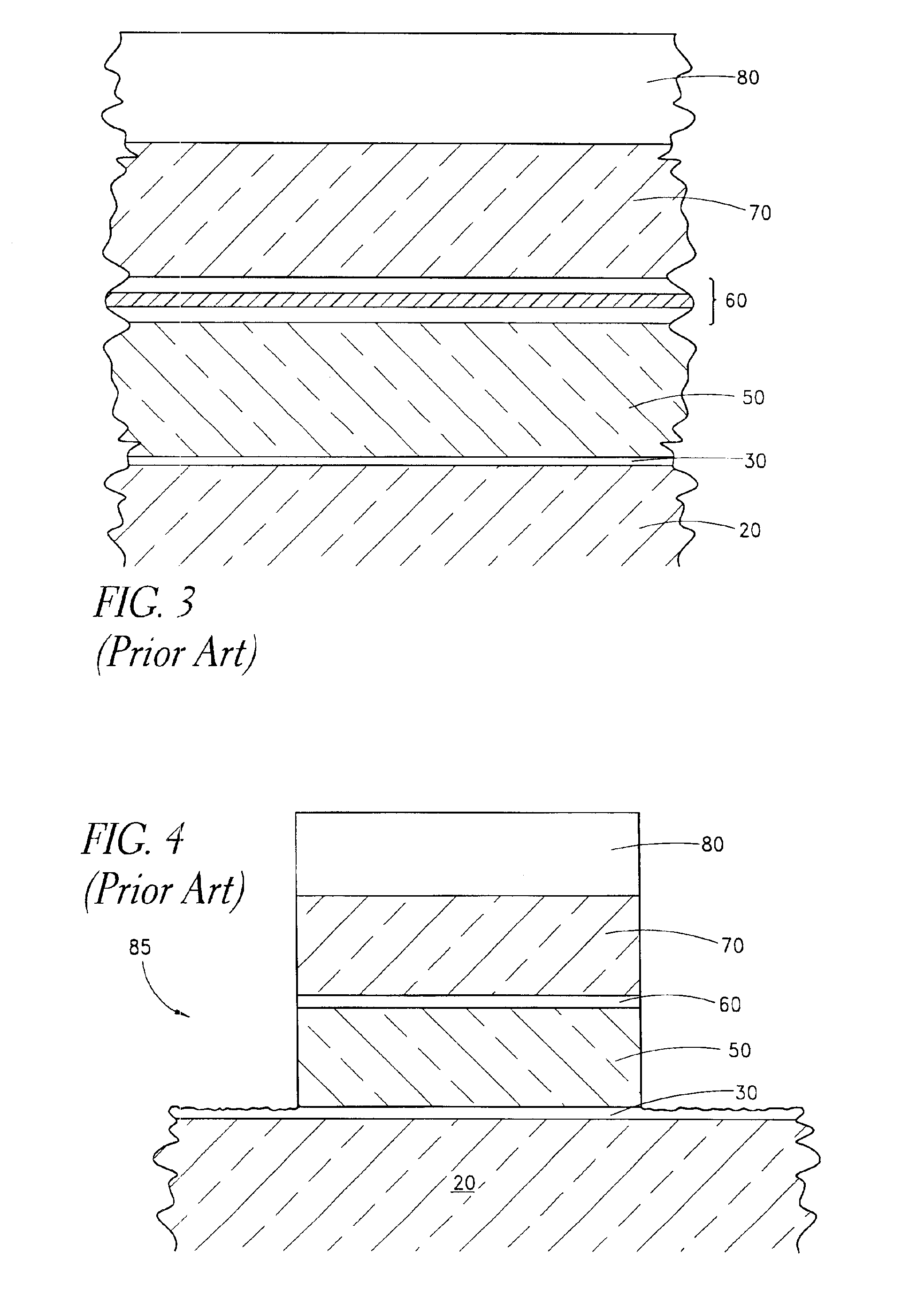
[0028]FIG. 1 illustrates an interim structure during the fabrication of an EEPROM transistor 10 in a flash memory cell constructed using prior art methods. The EEPROM transistor 10 includes a stacked gate structure 26 fabricated over a semiconductor substrate 20, which in the illustrated embodiments (and the prior art figures) is formed from the upper portion of a single-crystal silicon wa...


PUM


Abstract

The present invention provides a flash memory integrated circuit and a method for fabricating the same. The method includes etching a gate stack that includes an initial oxide layer directly in contact with a silicon layer, defining an oxide-silicon interface therebetween. By exposing the etched gate stack to elevated temperatures and a dilute steam ambient, additional oxide material is formed substantially uniformly along the oxide-silicon interface. Polysilicon grain boundaries at the interface are thereby passivated after etching. In the preferred embodiment, the interface is formed between a tunnel oxide and a floating gate, and passivating the grain boundaries reduces erase variability due to enhanced charge transfer along grain boundaries. At the same time, oxide in an upper storage dielectric layer (oxide-nitride-oxide or ONO) is enhanced in the dilute steam oxidation. Thermal budget can be radically conserved by growing thin oxide layers on either side of a nitride layer prior to etching, and enhancing the oxide layers by dilute steam oxidation through the exposed sidewall after etching. The thin oxide layers, like the initial tunnel oxide, serve as diffusion paths to enhance uniform distribution of OH species across the buried interfaces being oxidized.

Description

CLAIM OF PRIORITY[0001]This application is a divisional of U.S. patent application Ser. No. 09 / 648,699 filed Aug. 25, 2000 now U.S. Pat. No. 6,348,380, the disclosures of which are hereby incorporated in their entirety by reference herein.FIELD OF THE INVENTION[0002]The present invention generally relates to transistor gate dielectrics and methods of fabricating the same. More particularly, the invention relates to processes and structures for improving tunnel oxide quality in erasable programmable read-only memories (EEPROMs).BACKGROUND OF THE INVENTION[0003]Memory devices such as erasable programmable read-only memories (EPROMs), electrically erasable programmable read-only memories (EEPROMs), or flash erasable programmable read-only memories (FEPROMs) are erasable and reusable memory cells which are often used in digital cellular phones, digital cameras, LAN switches, cards for notebook computers, etc. A memory cell operates by storing electric charge (representing an “on” state)...

Claims


Application Information

Patent Timeline
Patent Type & Authority Patents(United States)
IPC IPC(8): H01L21/28H01L21/02H01L29/40H01L29/51
CPCH01L21/28273H01L29/511H01L29/517H01L29/40114
Inventor WEIMER, RONALD A.POWELL, DON C.MOORE, JOHN T.MCKEE, JEFF A.
Owner MICRON TECH INC
Learn More