Constant RON switch circuit with low distortion and reduction of pedestal errors

a constant ron, pedestal error technology, applied in the field of switch circuits, can solve the problems of low vdd level, low drive voltage or turn-on voltage, non-ideal behavior of the “on” resistance rsub>on /sub, increase the fabrication cost, etc., to achieve the effect of reducing the value of ron, reducing the distortion, and reducing the bandwidth

Inactive Publication Date: 2005-10-18
NAT SEMICON CORP
View PDF26 Cites 39 Cited by
  • Summary
  • Abstract
  • Description
  • Claims
  • Application Information

AI Technical Summary

Benefits of technology

[0014]Therefore, it is desirable to provide a switch circuit capable of operating at low Vdd levels with maximum bandwidth and minimum distortion. When a CMOS T-gate is used as the switch element, it is desirable to reduce t...

Problems solved by technology

One disadvantage is the lack of adequate drive voltages, or turn-on voltages, at low Vdd levels.
Even if there is sufficient drive capability, another disadvantage of conventional CMOS T-gates relates to the non-ideal behavior of the “on” resistance RON of the CMOS T-gate.
However, increasing the size of the T-gate not only increases the fabrication cost, it also increases the parasitic capacitance Cpar of the T-gate to a great extent.
However, reducing the threshold voltage of the transistors in order to reduce RON also has its limitation.
Therefore, at low Vdd levels, the transistors become depletion mode devices and lose the ability to be completely turned off.
Thus, neither of these prior art solutions are satisfactory at reducing RON.
When Vin is an AC or sinusoidal signal, this RON variation causes distortion in the output signal.
This RON variation places a fundamental limitation on the use of the conventional CMOS T-gates in high speed circuits, especially at low Vdd levels.
In summary, the two non-ideal characteristics of a conventional CMOS transmission g...

Method used


Image

  • Constant RON switch circuit with low distortion and reduction of pedestal errors
  • Constant RON switch circuit with low distortion and reduction of pedestal errors
  • Constant RON switch circuit with low distortion and reduction of pedestal errors

Examples


Embodiment Construction

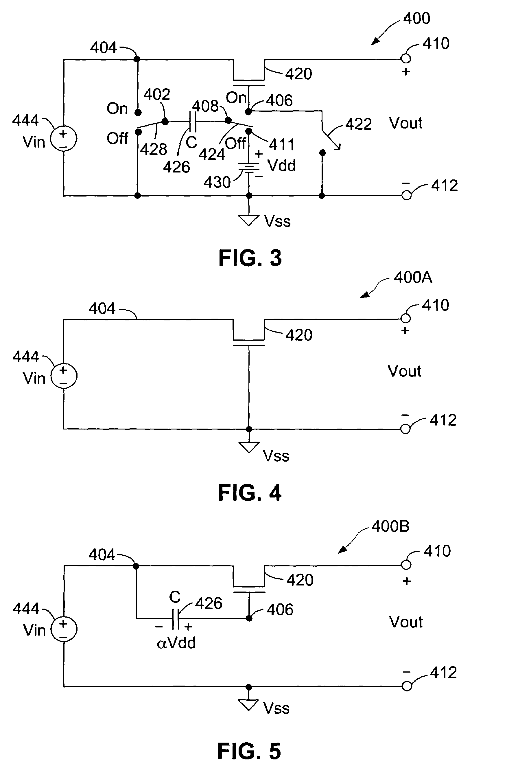
[0043]In accordance with the principles of the present invention, a self-bootstrapping constant RON switch circuit is provided. The switch circuit is capable of operating at Vdd levels as low as 2.0 volts with negligible distortion of the output waveform. FIG. 3 is a circuit diagram of a self-bootstrapping constant RON switch circuit 400 in accordance with one embodiment of the present invention. Referring to FIG. 3, switch circuit 400 includes an NMOS transistor 420 functioning as the main switching device. NMOS transistor 420 is an enhancement mode device having a threshold voltage value of less than 1 volt (typically 0.7 volts). The output voltage Vout of NMOS transistor 420 is provided at a node 410 with respect to ground node 412 (also called Vss). Output voltage Vout typically drives other circuitry such as a capacitive load CL (not shown).

[0044]Switch circuit 400 includes switches 422, 424 and 428, and a capacitor 426. Switches 422, 424 and 428 together with capacitor 426 ope...


PUM


Abstract

A low distortion, high frequency switch circuit for selectively coupling an input voltage terminal to an output voltage terminal includes a switching device coupled to the input voltage terminal and the output voltage terminal, a charge storage device, and a first, second and third switches. While the switch circuit is turned off, the charge storage device, typically a capacitor, is charged to a precharge voltage. Then, when the switch circuit is to be turned on, the charge storage device is coupled between the control terminal of the switching device and the input voltage terminal. As a result, the switching device receives a constant gate-to-source voltage approximately equals to the precharge voltage and becomes conductive with a minimum and constant RON for all values of input voltages. In another embodiment, the switch circuit includes a pedestal voltage compensation circuit for reducing charge injection induced pedestal errors.

Description

CROSS-REFERENCE TO RELATED APPLICATIONS[0001]This application is related to the following concurrently filed and commonly assigned U.S. patent applications: U.S. patent application Ser. No. 10 / 402,658, entitled “Digitizing Temperature Measurement System,” of Peter R. Holloway et al.; U.S. patent application Ser. No. 10 / 401,835, entitled “Low Noise Correlated Double Sampling Modulation System,” of Peter R. Holloway et al., now U.S. Pat. No. 6,750,796, issued on Jun. 15, 2004; and U.S. patent application Ser. No. 10 / 402,447, entitled “Constant Temperature Coefficient Self-Regulating CMOS Current Source,” of Peter R. Holloway et al. The aforementioned patent applications are incorporated herein by reference in their entireties.FIELD OF THE INVENTION[0002]The invention generally relates to a switch circuit. In particular, the present invention relates to a high frequency switch circuit having a constant “on” resistance and capable of operating at low power supply levels with little dist...

Claims


Application Information

Patent Timeline
IPC IPC(8): H03K17/00G11C27/02H03K17/06
CPCG11C27/02G11C27/024H03K17/063
Inventor HOLLOWAY, PETER R.
Owner NAT SEMICON CORP
Why Eureka
Try Eureka