Lithography system

Active Publication Date: 2005-10-25
ASML NETHERLANDS BV
View PDF4 Cites 320 Cited by
  • Summary
  • Abstract
  • Description
  • Claims
  • Application Information

AI Technical Summary

Benefits of technology

[0035]In an embodiment the transfer from the converter element in the control unit a region close to the modulation means achieved using optical fibers for the data transport. This allows flexible data transport with minimal disturbance by electromagnetic fields and other means. Furthermore, at allows the control unit to be located remote from the rest of the lithography system, for instance between 2-200 meters away from the rest of the system.
[0036]Currently, optical fibers that are used in telecom and Ethernet applications are optimized for specific wavelengths, predominantly 850, 1300 and 1500 nm. The 850 nm optimization is established due to the good availability of the standard InGaAs/GaAs laser diodes. The infrared wavelengths are used because of the low fiber transmission losses, typically smaller than 0.4 dB/km. Future developments aim for wavelengths of 660 and 780 nm. The lower wavelengths are preferred for the present invention because of fewer diffraction related limitations at these wavelengths. However, in some configurations larger wavelengths are desired. The wavelengths that can be used in the present invention range from about 200 to 1700 nm. Current developments furthermore make it possible to transfer multiple signals through one channel. For this purposes either multi-wav

Problems solved by technology

As the resolution becomes smaller and smaller, these masks have become more difficult to produce.
Furthermore, the (optical) means for projecting these masks have become very complex.
The switching of sources may get problematic when the switching speed increase

Method used


Image

  • Lithography system
  • Lithography system
  • Lithography system

Examples


example 1

Maskless Electron Beam Lithography System (FIG. 10)

[0113]In the maskless electron beam lithography system used in this example, the system comprises an aperture plate comprising electrostatic deflectors 21 to deflect incoming electron beamlets 22 passing through the apertures 23. This plate will be referred to as the beamlet blanker array 24. When the electron beamlets 22 have passed the beamlet blanker array 24 they will reach a second aperture array (beam stop array) 25 on which their trajectory will terminate when they are deflected.

[0114]The modulation concept of this lithography system is shown in FIG. 10. Incoming electron beamlets 22 are projected on the beamlet blanker array 24. The positions of the electron beamlets 22 correspond to the positions of the apertures 23 in the plate 24. The beamlet blanker plate 24 comprises a deflector element as modulation means. In this example said deflector element comprises an electrostatic deflector 21. Depending on the received informat...

example 2

Maskless Optical Lithography System (FIG. 13)

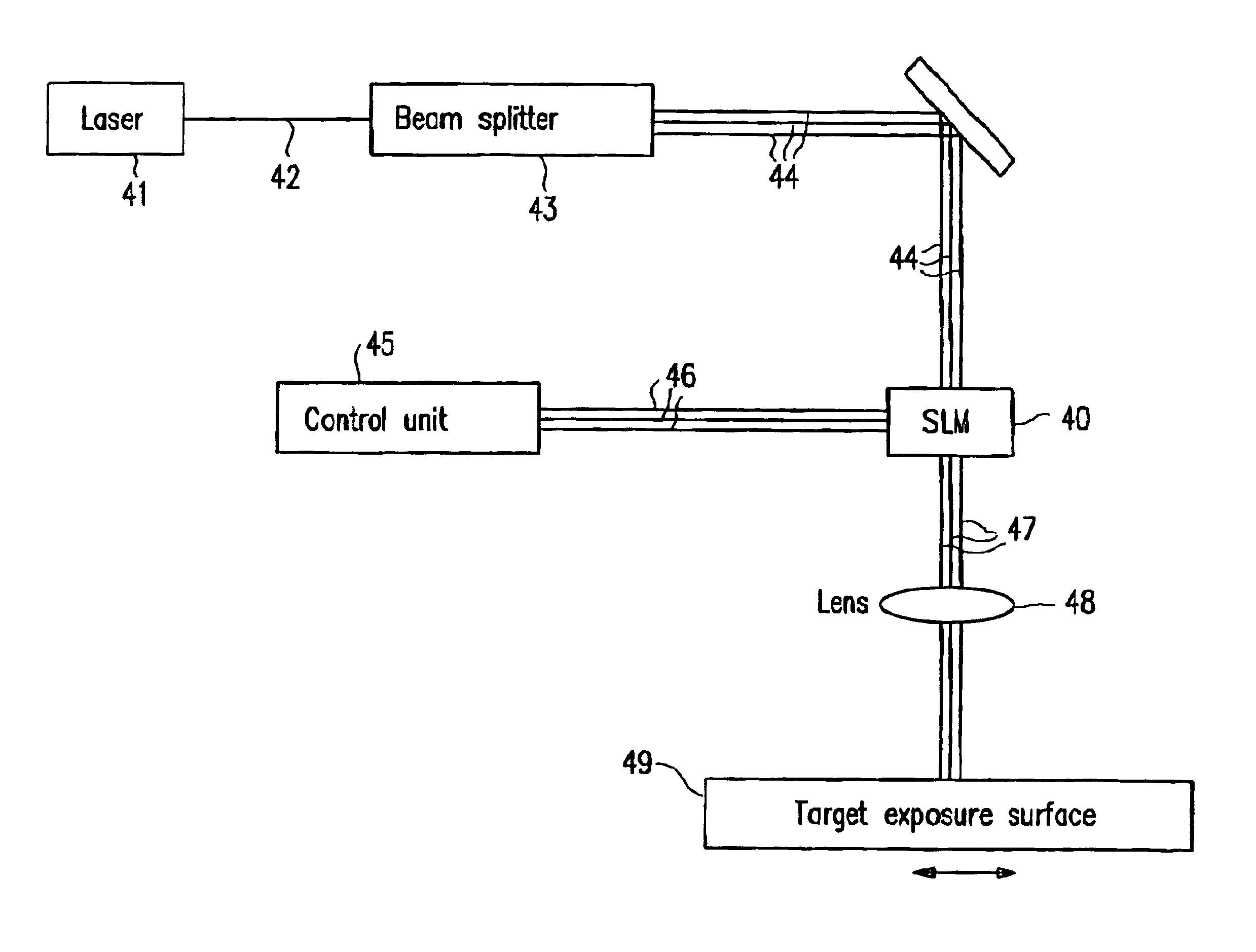
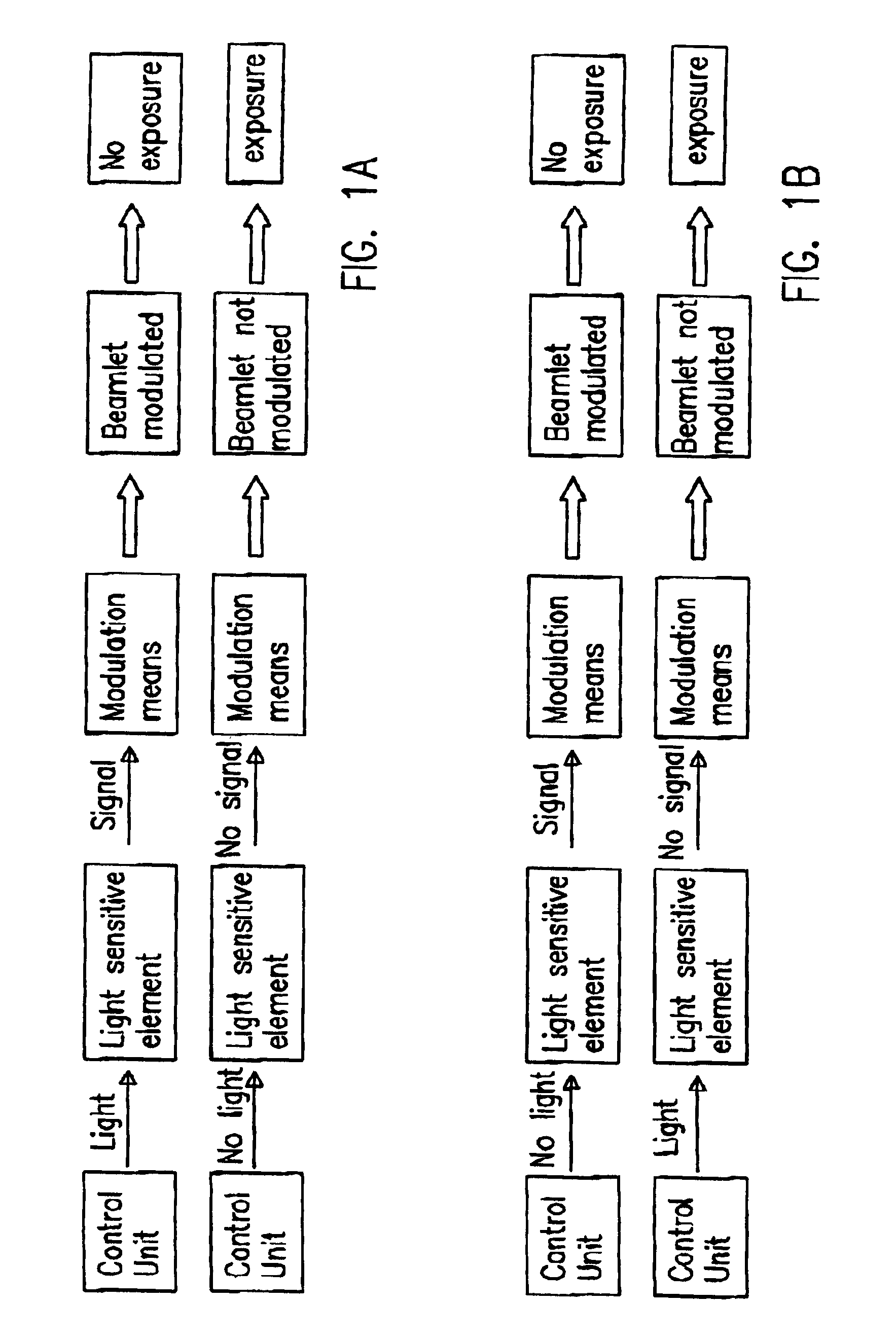
[0116]The maskless lithography system in this example comprises a spatial light modulator (SLM) 40. Maskless lithography systems using an SLM are in a general way disclosed in WO0118606. The SLM comprises an array of mirrors, which reflect the incoming light beams in such a way that the beam eventually is blanked or transmitted. An example of such an SLM is a deformable mirror device (DMD). A DMD is controlled in the same way as the electrostatic deflector array shown in the first example. The modulation signals couple into the system from the back or from the side.

[0117]One configuration is a backside control of the modulation. By providing the backside of each mirror with a light sensitive element, the control can be done with the use of the same optical carriers as mentioned before. Probably the use of free space optical interconnects is the most convenient option.

[0118]A schematic drawing of the operation is shown in FIG. 13. A laser ...


PUM


Abstract

A maskless lithography system for transferring a pattern onto the surface of a target. At least one beam generator for generating a plurality of beamlets. A plurality of modulators modulate the magnitude of a beamlet, and a control unit controls of the modulators. The control unit generates and delivers pattern data to the modulators for controlling the magnitude of each individual beamlet. The control unit includes at least one data storage for storing the pattern data, at least one readout unit for reading out the data from the data storage, at least one data converter for converting the data that is read out from the data storage into at least one modulated light beam, and at least one optical transmitter for transmitting the at least one modulated light beam to the modulation modulators.

Description

[0001]This is a non-provisional application claiming the benefit of Provisional application No. 60 / 421,464 filed Oct. 25, 2002.BACKGROUND[0002]Lithography systems, including ion, laser, EUV and electron beam systems, all require means to process and deliver a pattern to some kind of writing means. A well known way to accomplish this is by using a mask, and projecting this mask onto a substrate. As the resolution becomes smaller and smaller, these masks have become more difficult to produce. Furthermore, the (optical) means for projecting these masks have become very complex.[0003]A way of to overcome this problem is by using maskless lithography.[0004]Maskless lithography systems can be divided in two classes. In the first class the pattern data are sent towards the individual radiation source or sources. By tuning the intensity of the sources at the right times, a pattern can be generated on the substrate, which is most often a wafer or a mask. The switching of sources may get prob...

Claims


Application Information

Patent Timeline
IPC IPC(8): G03F7/20H01J37/317
CPCB82Y10/00G03F7/70825G03B27/52G03F7/70291G03F7/70508G03F7/70991H01J37/045H01J37/3174H01J37/3177G03F7/70383B82Y40/00H01J2237/0432H01J2237/0435H01J2237/0437H01J2237/2482G03F7/2006H01L21/0274G03F7/2008H01L21/0275
Inventor WIELAND, JAN-JACO MARCOVAN 'T SPIJKER, JOHANNES CHRISTIAANJAGER, REMCOKRUIT, PIETER
Owner ASML NETHERLANDS BV
Why Eureka
Try Eureka