Method of manufacturing a semiconductor device

Inactive Publication Date: 2005-11-08
SEMICON ENERGY LAB CO LTD
View PDF24 Cites 53 Cited by
  • Summary
  • Abstract
  • Description
  • Claims
  • Application Information

AI Technical Summary

Benefits of technology

[0020]With the construction described above, it becomes possible to shorten a time taken t

Problems solved by technology

Thus, processing efficiency is poor and it is an importan

Method used


Image

  • Method of manufacturing a semiconductor device
  • Method of manufacturing a semiconductor device
  • Method of manufacturing a semiconductor device

Examples


example 1

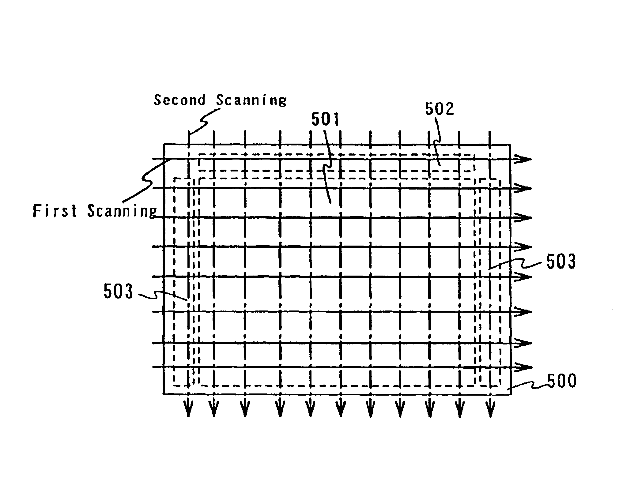
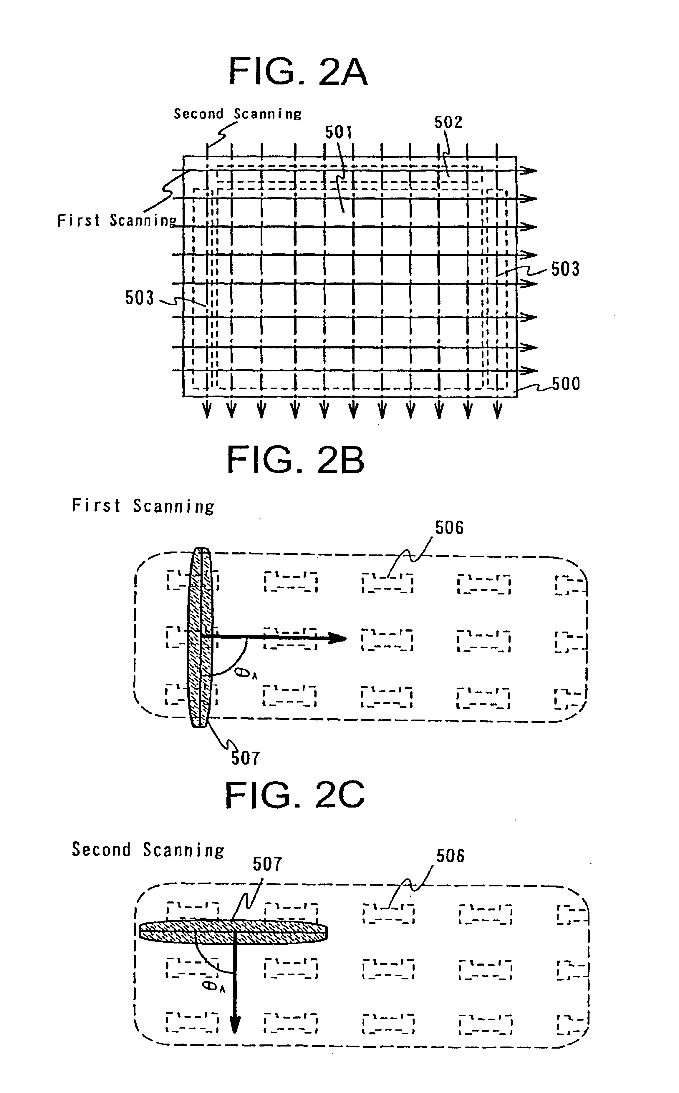
[0111]A crystalline semiconductor film formed through irradiation of a laser beam is composed of a plurality of crystal grains gathered together. The positions and the sizes of these crystal grains are random, and it is difficult to form a crystalline semiconductor film by specifying the positions and the sizes of the crystal grains. For this reason, an interface between crystal grains (grain boundary) may be present in an active layer formed by patterning the crystalline semiconductor film into an insular shape.

[0112]Different from the interior of the crystal grains, a myriad of recombination centers and trapping centers due to the amorphous structure and crystal defects are present at the grain boundary. It is known that when carriers are trapped in the trapping centers, the potential of the grain boundary rises, which erects a barrier with respect to the carriers and thereby deteriorates the current transport characteristic of the carriers. In a case where the grain boundary is p...

example 2

[0141]In the present example, an explanation will be given to the shape of a beam spot formed by a plurality of laser oscillating apparatuses of the invention.

[0142]FIG. 13(A) is a view showing one example of the shape of a beam spot of a laser beam oscillated from each of a plurality of laser oscillating apparatuses, formed on an object to be processed. The beam spot shown in FIG. 13(A) is of an elliptical shape. It should be appreciated, however, that in the laser apparatus of the invention, the shape of a beam spot of a laser beam oscillated from the laser oscillating apparatus is not limited to an elliptical shape. The shape of a beam spot varies with types of the laser, and can be formed by an optical system. For example, a laser beam emitted from a XeCl excimer laser (wavelength: 308 nm, pulse width: 30 ns) L3308 of Lambda Physik AG has a rectangular shape of 10 mm×30 mm (both being the half bandwidth in the beam profile). Also, a laser beam emitted from a YAG laser has a circ...

example 3

[0151]In the present example, an explanation will be given to an optical system used to obtain the beam spot shown in Example 2 above.

[0152]FIG. 15 shows a concrete arrangement of an optical system of the present example. FIG. 15(A) is a side view of the optical system in the laser apparatus of the invention, and a side view when viewed from the direction indicated by an arrow B of FIG. 15(A) is shown in FIG. 15(B). A side view when viewed in the direction indicated by an arrow A of FIG. 15(B) corresponds to FIG. 15(A).

[0153]FIG. 15 shows the optical system when four beam spots are synthesized into a single beam spot. It should be appreciated, however, that the number of beam spots to be synthesized in the present example is not limited to four, and the number of beam spots to be synthesized can be two to eight.

[0154]Numerals 401, 402, 403, 404, and 405 denote cylindrical lenses, and although it is not shown in FIG. 15, the optical system of the present example employs six cylindric...


PUM

PropertyMeasurementUnit
Angleaaaaaaaaaa
Angleaaaaaaaaaa
Thicknessaaaaaaaaaa

Abstract

To provide a continuous-oscillating laser apparatus capable of improving the efficiency of substrate treatment, a method of irradiating a laser beam, and a method of manufacturing a semiconductor device using the laser apparatus. Of the entire semiconductor film, a portion that needs to be left on the substrate after patterning is identified according to a mask. Then, a portion to be scanned by respective lasers are defined, so that a laser beam is irradiated twice in different scanning directions to a portion to be obtained at least through patterning and beam spots are impinged upon the scanned portion, thereby partially crystallizing the semiconductor film. In other words, in the invention, it is arranged in such a manner that a laser beam is not irradiated by scanning a laser beam across the entire semiconductor film but by scanning a laser beam twice at least to the absolutely necessary portion. According to the above arrangement, it is possible to save the time to irradiate a laser beam in waste to the semiconductor film at a portion to be removed through patterning, and the crystalline characteristics of the semiconductor film obtained after the patterning can be further enhanced.

Description

BACKGROUND OF THE INVENTION[0001]1. Field of the Invention[0002]The present invention relates to a laser processing apparatus and a laser irradiation method for crystallizing a semiconductor substrate, a semiconductor film or the like using a laser light or for performing activation after ion implantation, a semiconductor device formed by using the laser apparatus and a manufacturing method therefore, an electronic equipment using the semiconductor device, and a production system of the semiconductor device using the laser apparatus.[0003]2. Description of Related Art[0004]In recent years, a technique of forming a TFT on a substrate has greatly progressed, and its application and development for an active matrix semiconductor display device has been advanced. In particular, since a TFT using a poly crystalline semiconductor film has higher field-effect mobility (also referred to as a mobility) than a TFT using a conventional amorphous silicon film, it enables high speed operation. T...

Claims


Application Information

Patent Timeline
IPC IPC(8): B23K26/073B23K26/06H01L21/00H01L21/70H01L21/84G02F1/1368H01L21/20H01L21/268H01L21/336H01L21/77H01L29/786
CPCB23K26/0732B23K26/0736H01L21/2026H01L21/67282H01L21/67294H01L27/1285H01L21/02683H01L21/02422H01L21/02488H01L21/02502H01L21/0242H01L21/02672H01L21/02425H01L21/02686H01L21/02678H01L21/02532H01L21/02381H01L21/02691
Inventor YAMAZAKI, SHUNPEIOHTANI, HISASHIHIROKI, MASAAKITANAKA, KOICHIROSHIGA, AIKOSHIMOMURA, AKIHISAAKIBA, MAI
Owner SEMICON ENERGY LAB CO LTD
Why Eureka
Try Eureka