Avalanche photo-detector with high saturation power and high gain-bandwidth product

a photodetector and high saturation power technology, applied in the field of photodetectors, can solve the problems of serious bandwidth and output electrical power degradation, and achieve the effects of reducing device capacitance, operating voltage, carrier transport time and dark current, and increasing response speed and output power

Inactive Publication Date: 2005-11-08
IND TECH RES INST
View PDF7 Cites 35 Cited by
  • Summary
  • Abstract
  • Description
  • Claims
  • Application Information

AI Technical Summary

Benefits of technology

[0007]The object of the present invention is to provide an APD formed of IV-based or III-V based materials for reducing device capacitance, operating voltage, carrier transport time and dark current as well as increasing response speed and output power.
[0008]To achieve the object of the present invention, an avalanche photo-detector (APD) with high saturation power, high gain-bandwidth product, low noise, fast response, low dark current is provided. The APD of the present invention includes an absorption layer, a multiplication layer, a drift layer sandwiched between the absorption layer and the multiplication layer, and a field buffer layer sandwiched between the drift layer and the multiplication layer. The absorption layer is made of a first semiconductor to absorb incident light for converting the incident light into carriers and is graded heavily doped to produce a built-in electric field and solve the problems of photo-generated hole transport. In traditional APD, the photo-absorption layer is undoped to increase the electric field inside and reduce the transport time of photo-generated hole. However, under high optical power illumination, the photo-generated hole will result in serious bandwidth and output electrical power degradation. The doped photo-absorption layer technique of p-i-n photodetector structure is disclosed in U.S. Pat. No. 5,818,096. By use of the p-type doping in photo-absorption layer, the photo-generated hole can relax to the contact directly and output saturation power can be improved significantly. The multiplication layer is made of an undoped second semiconductor to receive carriers for multiplying current. The field buffer layer is a doped third semiconductor sandwiched between the absorption layer and the multiplication layer for concentrating the electric field in the multiplication layer when a bias voltage is applied. The drift layer is an undoped fourth semiconductor sandwiched between the field buffer layer and the absorption layer for capacitance reduction.

Problems solved by technology

However, under high optical power illumination, the photo-generated hole will result in serious bandwidth and output electrical power degradation.

Method used


Image

  • Avalanche photo-detector with high saturation power and high gain-bandwidth product
  • Avalanche photo-detector with high saturation power and high gain-bandwidth product
  • Avalanche photo-detector with high saturation power and high gain-bandwidth product

Examples


Embodiment Construction

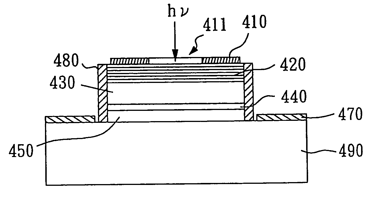
[0020]The inventive APD can optionally include a first conduction layer and a second conduction layer in order to connect and conduct the absorption layer or the multiplication layer. In general, the absorption layer of the APD of the present invention is sandwiched between the first conduction layer and the drift layer. The multiplication layer is sandwiched between the second conduction layer and the field buffer layer. The absorption layer of the APD is graded doped, to produce a built-in electric field. An example of p-type Si absorption layer is given. The doping concentration for the p-type Si absorption layer is gradually reduced from a surface of an epi layer to a bottom of the epitaxy layer. As compared to traditional APD structure, our heavily doped p-type photo-absorption layer will not be depleted during operation, and the photo-generated hole can relax to the contact directly. The APD can also optionally include a t waveguide epi-layer structure. The absorption layer is...


PUM


Abstract

An avalanche photo-detector (APD) is disclosed, which can reduce device capacitance, operating voltage, carrier transport time and dark current as well as increasing response speed and output power. Thus, an avalanche photo-detector (APD) with high saturation power, high gain-bandwidth product, low noise, fast response, low dark current is achieved. The APD includes an absorption layer with graded doping for converting an incident light into carriers, an undoped multiplication layer for multiplying current by means of receiving carriers, a doped field buffer layer sandwiched between the absorption layer and the multiplication layer for concentrating an electric field in the multiplication layer when a bias voltage is applied, and an undoped drift layer sandwiched between the absorption layer and the field buffer layer for capacitance reduction.

Description

BACKGROUND OF THE INVENTION[0001]1. Field of the Invention[0002]The present invention relates to a photodetector and, more particularly, to an avalanche photodetector (APD) adapted for high-speed long-distance optical fiber communication.[0003]2. Description of Related Art[0004]Recently, APDs have become the leading device in photo-receiver market in 2.5 GHz or 10 GHz bandwidth for optical communication. Compared with fast p-i-n photodetectors, APD can provide higher sensitivity and gain in the desired bandwidth. As compared to photo-transistors (HPTs) with the same gain, APDs are preferred in its speed potential and short falling time of impulse response, such that they are more practical in eye-diagram test and commercial optical communication than HPTs do. When a high-speed photodetector is developed in a market of high-speed long-distance optical fiber communication, two factors of high output power-bandwidth product and high efficiency-bandwidth product need to be met. However,...

Claims


Application Information

Patent Timeline
Patent Type & Authority Patents(United States)
IPC IPC(8): H01L31/102H01L31/107H01L31/08
CPCB82Y10/00H01L31/107
Inventor SHI, JIN-WEILIU, CHEE-WEE
Owner IND TECH RES INST
Why Eureka
Try Eureka