

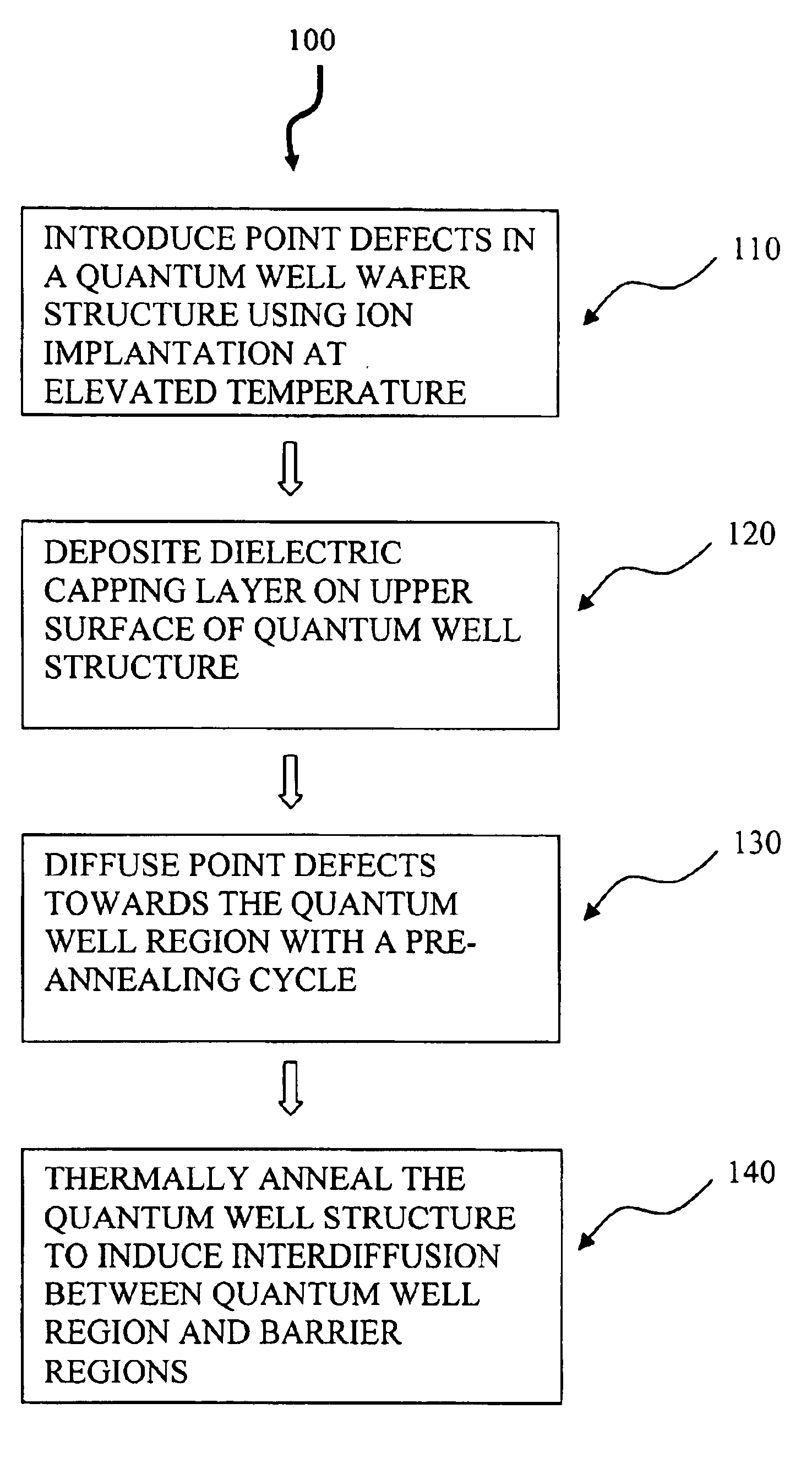
Method for quantum well intermixing using pre-annealing enhanced defects diffusion
a quantum well and diffusion method technology, applied in semiconductor lasers, nanooptics, laser details, etc., can solve the problems of low production yield to the final device, point defects can move around in the crystal structure, and the integration of multiple photonic elements using these complex techniques is complicated, etc., to achieve enhanced defects diffusion disordering and low polarization sensitive
- Summary
- Abstract
- Description
- Claims
- Application Information
AI Technical Summary
Benefits of technology
Problems solved by technology
Method used
Image

Examples
process examples
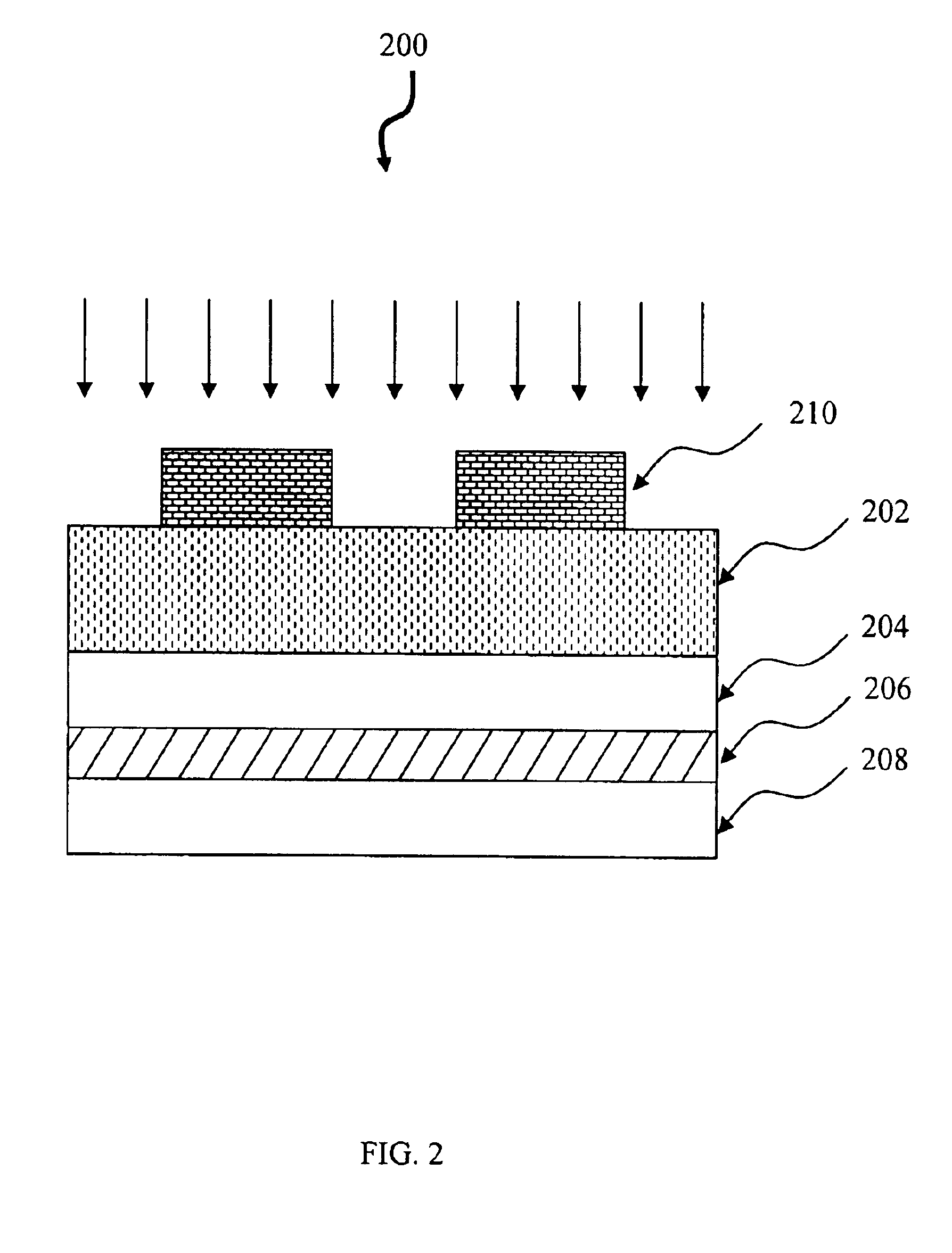
[0062]The following are examples of the fabrication of 2-bandgap and multiple-bandgap semiconductor devices according to the present invention. The following examples include process parameters such as layer composition and thickness, and well as anneal temperature and times. These parameter values are provided as examples only, and should not be deemed to limit the scope of the present invention. The example quantum well structure 200 used in these exemplary processes is shown in FIG. 4 and in the following table:
[0063]
ElementThicknessConcentrationNumber(Å)MaterialDopant(cm−3)Remark2241000In0.53Ga0.47AsZincp = 2 × 10¹⁹Metal Contact22214000InPZincp = 5 × 10¹⁷Upper cladding220700GaxIn1−xAsyP1−y—IntrinsicUpper SCH(λg = 1.18 μm)Confinementlattice matchedLayer204140Ga0.54In0.46As—IntrinsicCore 226, which(tensile strained)includes five206 67 × 5Ga0.2In0.8As0.7P0.3—IntrinsicGa0.2In0.8As0.7P0.3(compressive strained)quantum well208140 × 5Ga0.54In0.46As—Intrinsiclayers separated(tensile stra...
example 1
2-Bandgap Semiconductor Chip
[0068]FIGS. 5A-5C illustrate a process for the fabrication of a 2-bandgap semiconductor device. The process begins after the quantum well structure 200 shown in FIG. 4 has been formed. An implant masking layer 228 (e.g., 1000 nm of SiO2) is first deposited on the QW structure 200. Selective bandgap tuning windows 230 are formed in the masking layer 228 using a standard lithography process (photolithography or e-beam lithography, etc). Specifically, a photo-resist layer 232 is formed over the masking layer 228, where portions of the photo resist layer 232 are then removed from the regions in which the windows 230 are to be formed, leaving portions of the masking layer 228 exposed. Wet or dry SiO2 etching techniques are then used to remove the exposed portions of the masking layer 228, leaving windows 230 formed in the masking layer 228 that expose portions of the underlying QW structure 200, as illustrated in FIG. 5A. The remainder of the structure include...
example 2
Multiple-Bandgap Engineering Process
[0075]A multiple bandgap tuning technique is next illustrated, which is similar to the process used in the example above, but it fabricates a triple bandgap quantum well chip. In this example, depicted in FIGS. 7A and 7B, the patterned implant mask 228 (e.g., SiO2) is formed not only with window regions 230 in which the mask material is completely removed, but also with semi window regions 240 in which the mask material is partially removed with varying thicknesses, where the thicknesses allow varying degrees of the ions to penetrate therethrough into the underlying cladding layer 222. The manufacturing of the SiO2 implantation mask with different thicknesses can be achieved using a single or a multiple step lithography / etch process. For example, the implant mask layer 228 is first coated with a layer of photo resist, and a photolithography / etch process (wet or dry) is used to define window regions 230 in which the mask material is removed to expo...
PUM
 Abstract
Description
Claims
Application Information