Connector-integrated type polymer optical waveguide, method and mold for producing the same

a technology of integrated type and optical waveguide, which is applied in the direction of optical waveguide light guide, instruments, optics, etc., can solve the problems of inability to obtain a sufficiently large difference in refractive index between the core layer and the clad layer, and the precision of the obtained core diameter is expensive, etc., to achieve easy and inexpensive production, excellent structure stability, and less number of processes

Inactive Publication Date: 2006-01-24
FUJIFILM BUSINESS INNOVATION CORP
View PDF10 Cites 21 Cited by
  • Summary
  • Abstract
  • Description
  • Claims
  • Application Information

AI Technical Summary

Benefits of technology

[0026]In consideration of the above-mentioned problems, the present invention provides a connector-integrated type polymer optical waveguide with excellent structure s

Problems solved by technology

However, the selective polymerization method (1) has a problem in the lamination process, the methods (2) and (3) are costly because of the employment of the photolithography, and the method (4) has a problem in the precision of the diameter of the obtained core.
Further, the method (5) has a problem that sufficiently large difference in refractive index cannot be obtained between the core layer and the clad layer.
Presently, the practically applicable methods are only the methods (2) and (3) and even these methods have the above-mentioned problem, in terms of the cost.
None of the methods (1) to (5) is satisfactorily applicable to formation of a polymer optical waveguide on a flexible plastic substrate having a large surface area.
Consequently, there arises a problem in that the light leaks out through the thin layer.
However, since the method uses the monomer as the core formation material, there arises a problem in that the volume shrinkage rate at the time when the monomers are polymerized to be a polymer is large and the transmission loss in the polymer optical waveguide is high.
Also, the method is a somewhat troublesome method including the processes of fixing the patterned substrate and the flat substrate by a clamp and, in addition to that, sealing the contact part thereof with a resin.
In short, this method is unsuitable for mass production and, as a result, cost down cannot be achieved.
Further, it is impossible for this method to be applied to production of a polymer optical waveguide using a film whose thickness is of mm order or a film whose thickness of 1 mm or less as a clad.
However, when the above-mentioned patent of Enoch et al. is applied to pro

Method used


Image

  • Connector-integrated type polymer optical waveguide, method and mold for producing the same
  • Connector-integrated type polymer optical waveguide, method and mold for producing the same
  • Connector-integrated type polymer optical waveguide, method and mold for producing the same

Examples


example 1

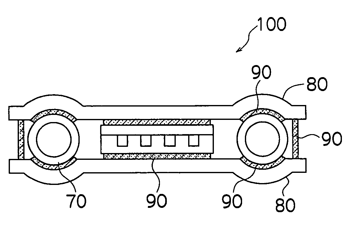
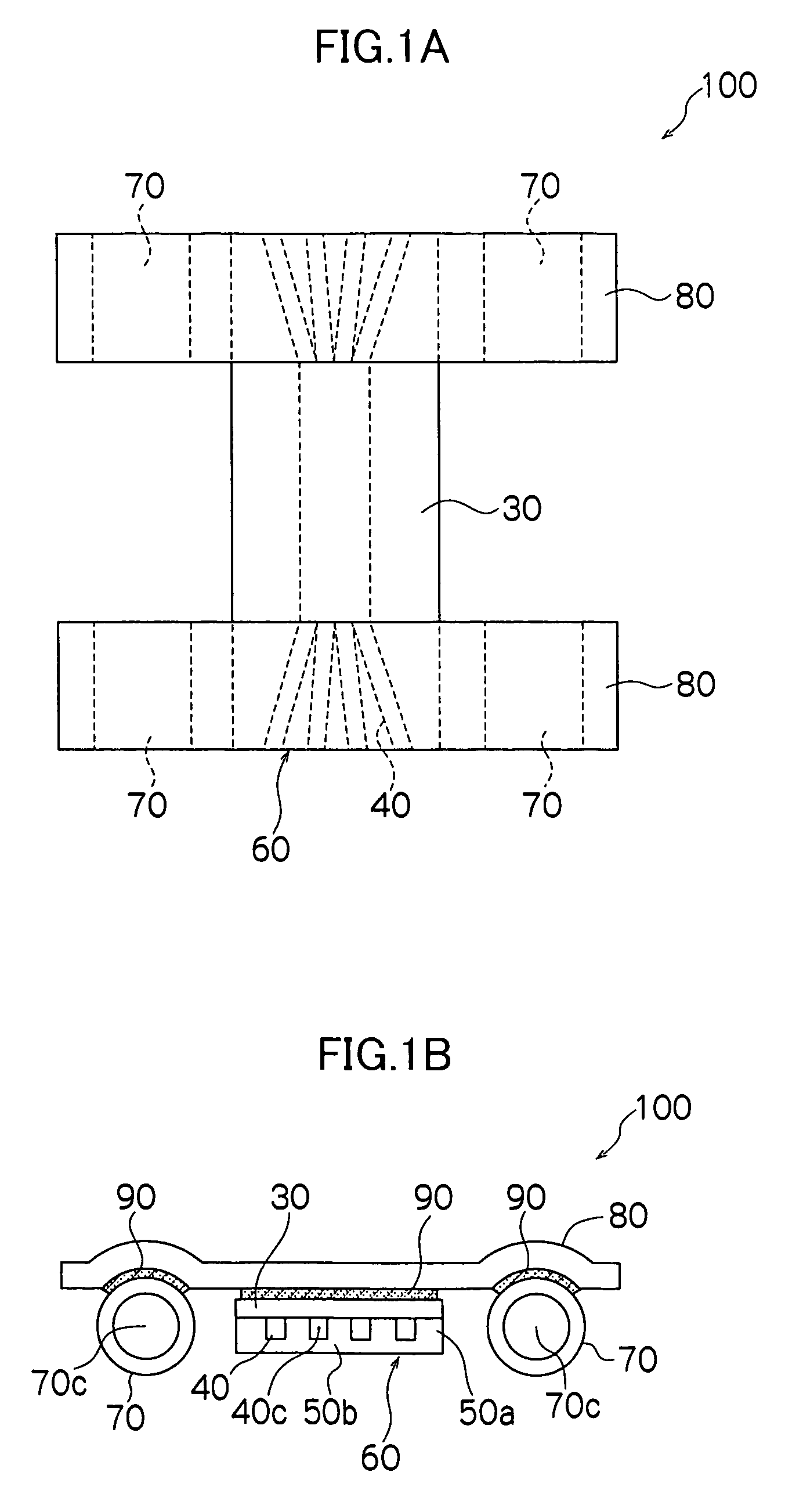
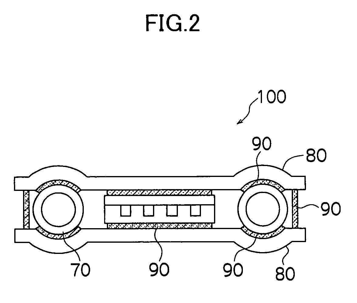
[0176]In this example, a connector-integrated type polymer optical waveguide having 4×4 branched optical waveguide core, as shown in FIGS. 1A and 1B, is produced.

[0177]At first, a resist as a thick film (SU-8 manufactured by Micro Chemical Co., Ltd.) is applied to a Si substrate by a spin coating method. Thereafter, the resist is prebaked at 80° C. and exposure through a photomask and development are effected, whereby: a projected portion corresponding to the 4×4 branched optical waveguide core [the cross-sectional area at the branched portion thereof is a square of 50 μm×50 μm, the cross sectional area of the projected portion at the mixing portion is a rectangle of 200 μm×10 mm, the pitches (i.e., the pitches of the projected portions at the positions corresponding to the core position observed at the cross-section obtained by cutting with a dicing saw, which will be described later) are 250 μm, and the length of the projected portion is the sum of the length of the dicing saw-cut...

example 2

[0193]A connector-integrated type polymer optical waveguide is produced in a manner similar to that of Example 1, except that the rigid member for connector formation made of a stainless steel is set not at both upper and lower sides but only at one side (refer to FIG. 5D). The average insertion loss at the initial stage is 3 dB in such a structure, and the cost is significantly reduced, as compared with Example 1. However, as the average insertion loss is increased to 4 dB under the conditions of 70° C. temperature and 95% humidity, it is assumed that this structure is suitable for a connector used at the room temperature.

example 3

[0194]Connector-integrated type polymer optical waveguides are produced in a manner similar to that of Example 1, except that the material of the rigid member of connector formation (a stainless plate in Example 1) is replaced with one of: a mixture of an epoxy resin and 70% by weight of a metal powder; a mixture of an epoxy resin and 70% by weight of glass; glass; and a ceramic sintered body, and that the two-component-mixing type epoxy resin is used as the adhesive for fixation.

[0195]Connector-integrated type polymer optical waveguides which achieve substantially the same performances as that of Example 1 are obtained. Further, in order to reduce cost, other connector-integrated type polymer optical waveguides are produced in a manner similar to that of Example 3, except that an aluminum die cast is used. In this case, the performances at the room temperature are substantially the same as those of Example 1. However, the insertion loss at a high temperature is increase to 3.4 dB.


PUM


Abstract

The present invention provides a connector-integrated type polymer optical waveguide, comprising: an optical waveguide including a film substrate for clad, an optical waveguide core provided on the film substrate, and a clad layer formed on side faces and a top face of the core; a pair of connector sleeves formed at positions at which the connector sleeves sandwich the optical waveguide core at least in one end portion of the polymer optical waveguide; and a rigid member for connector formation, wherein the film substrate for clad and the connector sleeves are fixed to the rigid member for connector formation in such a state that the center of the optical waveguide core and the center for connector sleeves are substantially on the same plane. The present invention also provides a method for producing the above-mentioned connector-integrated type polymer optical waveguide and a mold to be used for the method.

Description

CROSS-REFERENCE TO RELATED APPLICATION[0001]This application claims priority under 35 USC 119 from Japanese Patent Application No. 2003-166485, the disclosures of which are incorporated by reference herein.BACKGROUND OF THE INVENTION[0002]1. Field of the Invention[0003]The present invention relates to a connector-integrated type polymer optical waveguide and a method of producing the optical waveguide.[0004]2. Description of the Related Art[0005]The following methods have been proposed as a polymer optical waveguide production method: (1) a method (selective polymerization method) of impregnating a film with a monomer, selectively exposing the core portion of the film for changing the refractive index thereof, and forming a laminate by using the film; (2) a method (RIE method) of forming a core layer and a clad layer by coating and then forming a clad portion by reactive ion etching; (3) a photolithographic method (direct exposure method) of carrying out exposure and development by ...

Claims


Application Information

Patent Timeline
IPC IPC(8): G02B6/12G02B6/122G02B6/13G02B6/38G02B6/42G02B6/43
CPCG02B6/1221G02B6/3882G02B6/43G02B6/4206G02B6/4292G02B6/3885
Inventor SHIMIZU, KEISHIOHTSU, SHIGEMIYATSUDA, KAZUTOSHIAKUTSU, EIICHI
Owner FUJIFILM BUSINESS INNOVATION CORP
Why Eureka
Try Eureka