Optical waveguide and method for fabricating the same

a technology of optical waveguides and core segments, applied in the field of optical components, can solve the problems of long processing time, uneven distribution of dopant in a direction, and long time-consuming, and achieve the effects of easy production of optical waveguides, good mass production productivity, and constant precision in the shape of core segments

Inactive Publication Date: 2006-02-07
PANASONIC CORP
View PDF16 Cites 52 Cited by
  • Summary
  • Abstract
  • Description
  • Claims
  • Application Information

AI Technical Summary

Benefits of technology

[0011]Since this makes possible to bond directly between the core segment and the lower cladding layer by using glass materials having different refraction factors and different coefficients of thermal expansion, it realizes good optical characteristics at their interface and increases bonding strength. In addition, the optical waveguide can be produced at even a lower temperature as compared to the prior art method when the upper cladding layer is formed with the sputtering method, thereby realizing not only improvement of flexibility in selecting the materials but also reduction of the cost.
[0023]Moreover, a method of manufacturing an optical waveguide includes the step of direct bonding only after both bonding surfaces of the lower cladding layer and the core layer are polished to 0.1 nm to 1 nm in arithmetic mean surface roughness (Ra) and 0.1 μm to 1 μm in flatness throughout the entire surface areas of the substrate being bonded. This method can thus ensure the direct bonding over the entire surfaces even though it uses a substrate of 3 inches or larger In diameter, for instance, so as to allow manufacturing of optical waveguides with high productivity. In this method, 1 nm or less in the surface roughness Ra can establish reliable interatomic bonding between glass components of the substrate, and 1 μm or less in flatness can make uniform contact of the substrate over the entire surface areas, thereby ensuring reliability and consistency In the direct bonding.

Problems solved by technology

However, there exists the following problems In the deposition method and the Ion exchange method described above.
Although the optical waveguide formed by the deposition method shows the smallest transmission loss, it has a problem in productivity because It requires many processes to make the optical waveguide as It must go through the deposition and sintering processes for the core segments and the cladding layer, and the patterning process using the photolithography method, each of which requires a long duration of processing time.
On the other hand, although the optical waveguide can be formed In a comparatively short time with the ion exchange method, It produces uneven distribution of the dopant in a direction of thickness of the glass substrate because the core layer is formed by ion exchange.
This consequently produces uneven variation of refraction factor in the direction of thickness and increases the transmission loss, thereby giving rise to a problem.

Method used


Image

  • Optical waveguide and method for fabricating the same
  • Optical waveguide and method for fabricating the same
  • Optical waveguide and method for fabricating the same

Examples


first exemplary embodiment

[0028](First Exemplary Embodiment)

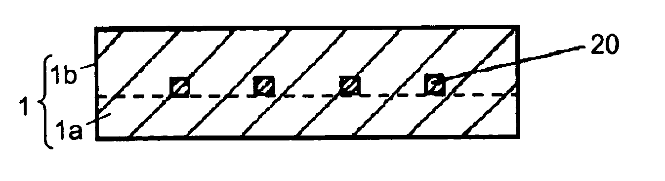
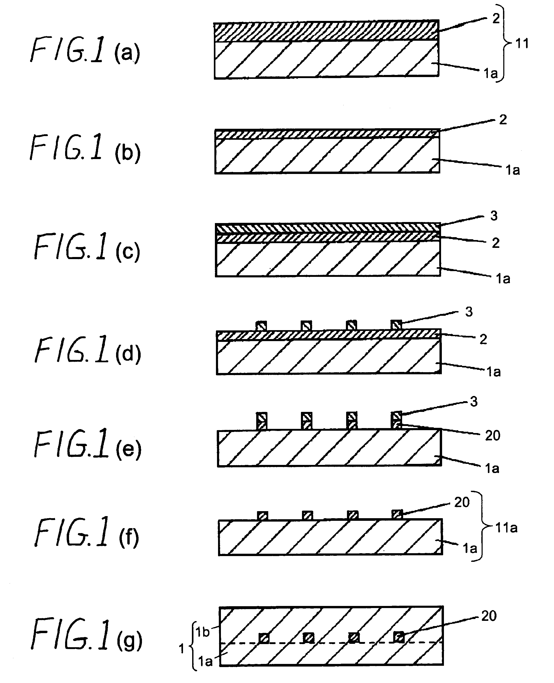
[0029]FIGS. 1(a)-(g) illustrates processing diagrams for manufacturing an optical waveguide according to the first exemplary embodiment of the present invention. A circular shape fluorine crown glass of 3 inches in diameter, as a substrate constituting lower cladding layer 1a, and a borosilicate crown glass of the same shape, as another substrate constituting core layer 2 were directly bonded together. FIG. 1(a) shows an appearance of the bonded state. The direct bonding is made in the following manner. First, one surface of each of the glass substrates is optically polished to such an extent that it becomes 1 nm in arithmetic mean surface roughness (Ra) and 1 μm in flatness. After that, these glass substrates are rinsed to a level of cleanliness that a contact angle of water to these glass substrates is 5 degrees or less. Next, after the polished surfaces of these glass substrates are abutted and pressed against each other, they are heat-treated at...

second exemplary embodiment

[0046](Second Exemplary Embodiment)

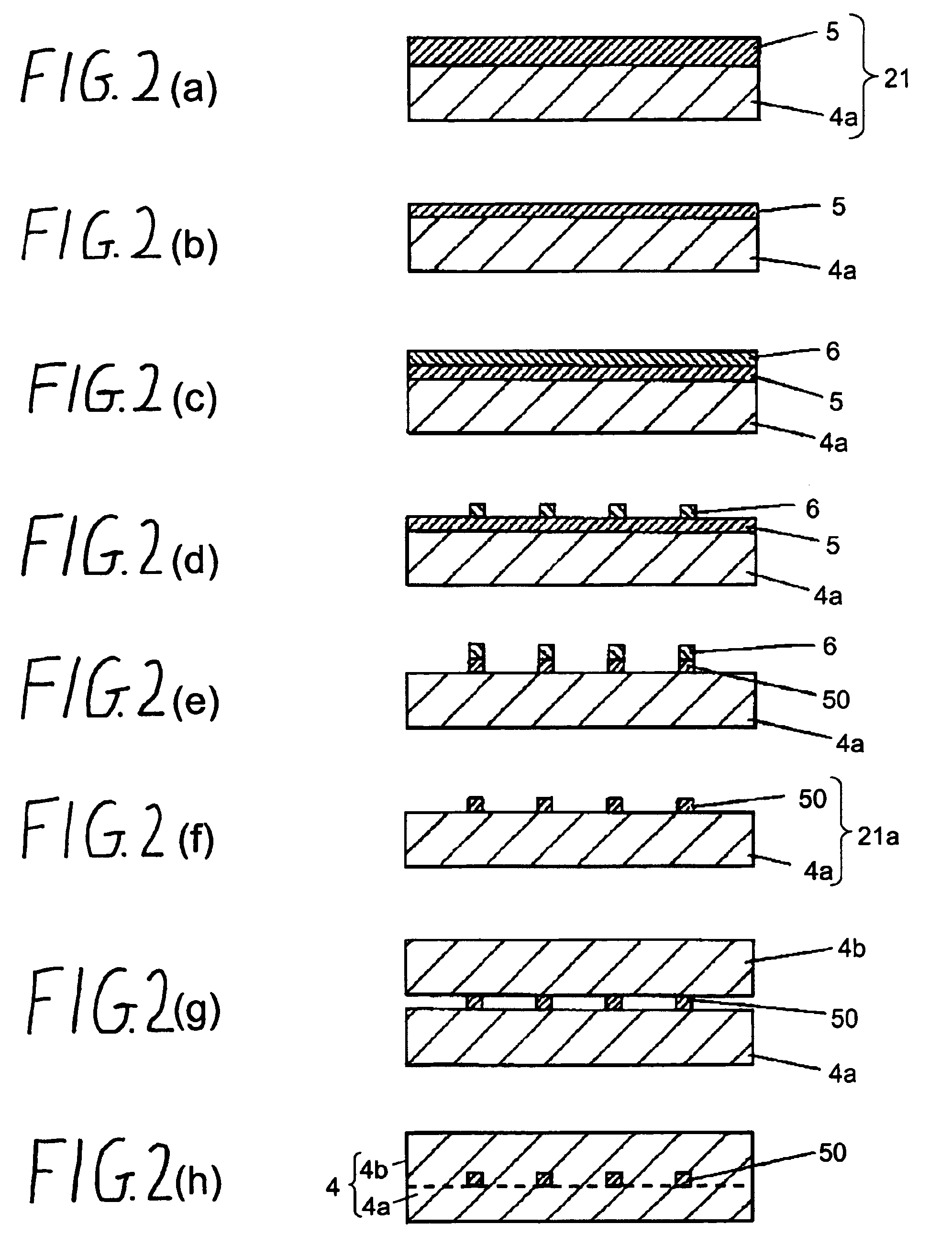
[0047]FIGS. 2(a)-(h) illustrates processing diagrams for manufacturing an optical waveguide according to the second exemplary embodiment of the present invention. A circular shape fluorine crown glass of 3 inches in diameter, as a substrate constituting lower cladding layer 4a, and another fluorine crown glass of the same shape, as a substrate constituting core layer 5 were put together by direct bonding. FIG. 2(a) shows an appearance of the bonded state. The method of making the direct bonding is the same as that described in the first exemplary embodiment, and details are therefore skipped. Bonding directly the core layer 5 and the lower cladding layer 4a obtains bonded substrate 21 in which the core layer 5 and the lower cladding layer 4a are Integrated into one body.

[0048]Next, a surface of the core layer 5 is ground and polished until a thickness of the core layer 5 becomes 5 to 7 μm, as shown in FIG. 2(b). The core layer 5 is then coated with...


PUM

PropertyMeasurementUnit
Raaaaaaaaaaa
mean surface roughnessaaaaaaaaaa
arithmetic mean surface roughnessaaaaaaaaaa

Abstract

An optical waveguide comprising cladding 1 and core segment 20 buried in cladding 1 and serving as a waveguide, wherein a combination of glass material constituting the core segment 20 and another glass material constituting the cladding 1 is so selected that an absolute value of difference in coefficient of thermal expansion between these materials (α1-α2) is within a range of 0 and 9×10⁻⁷° C., where α1 denotes a coefficient of thermal expansion of the former material and α2 denotes that of the latter material. Since this makes possible to bond directly the glass materials having different refraction factors and different coefficients of thermal expansion, and to produce the optical waveguide at even a lower temperature as compared to the prior art method as an upper cladding layer is formed with the sputtering method, it realizes reduction in number of processes and time of manufacture, thereby providing the optical waveguide of low transmission loss at low cost, as well as a method of manufacturing the same.

Description

[0001]This application is a U.S. National Phase Application of PCT International Application PCT / JP02 / 09574.FIELD OF THE INVENTION[0002]The present invention relates to an optical component, and in particular, it relates to an optical waveguide and a method of manufacturing the same.BACKGROUND OF THE INVENTION[0003]In optical components of a waveguide system such as optical splitters, optical combiners, optical dividers, optical multiplexers and the like, there hitherto are numerous methods of forming optical waveguides on a substrate, which can be categorized generally into two groups that are deposition method and ion exchange method.[0004]Deposition method is the method of forming an SiO2 film on a substrate made of silicon and the like, and it includes the flame hydrolysis deposition method, the plasma assisted chemical vapor deposition method (P-CVD method), the molecular beam epitaxy method (MBE method), and the like, to be more specific.[0005]Referring now to FIG. 3(a)-(c), d...

Claims


Application Information

Patent Timeline
Patent Type & Authority Patents(United States)
IPC IPC(8): G02B6/00C03B37/022C03B37/075G02B6/10G02B6/02G02B6/12G02B6/132G02B6/138G02B6/25
CPCG02B6/02042G02B6/10G02B6/12G02B6/138G02B6/25G02B6/132G02B2006/12176
Inventor HIRAKA, MASAHIROFURUKAWA, SHIGEO
Owner PANASONIC CORP
Why Eureka
Try Eureka