
Circuit element having a first layer composed of an electrically insulating substrate material, a method for producing a circuit element, bispyridinium compounds and their use in circuit elements

a technology of bispyridinium compounds and circuit elements, which is applied in the field of circuit elements having a first layer composed of an electrically insulating substrate material, bispyridinium compounds and their use in circuit elements, can solve the problems of low signal, two circuit elements which are known from [1] and [2] have further disadvantages for widescale practical use, and the suitability of langmuir-blodgett methods for the coating of components such as silicon wafers, normally

Inactive Publication Date: 2006-02-14
QIMONDA
View PDF8 Cites 9 Cited by
  • Summary
  • Abstract
  • Description
  • Claims
  • Application Information

AI Technical Summary

Benefits of technology

[0061]It is thus possible to simplify the electron release by the bispyridinium unit, for example by substituents R which are rich in electrons, such as alkyl or alkyl residues, which exert an inductive, electron-donating effect (referred to as the +I effect), and in this way decrease the reduction potential. The same is true for substituents which place free electron pairs at disposal and allow the formation of resonance structures, i.e. which show an +M effect. Examples of such substituents are —OH, —OR, —NH2, —NHR, —SR or fluorine.
[0062]Effects in the opposite sense, i.e. increasing the oxidation potential, can be achieved by substituents with electron-withdrawing −I and −M effects (for example —CN, —NO2, —COOH, —SO3H) or substituents such as chlorine, in which an electron-withdrawing effect prevails over an electron-donating effect.
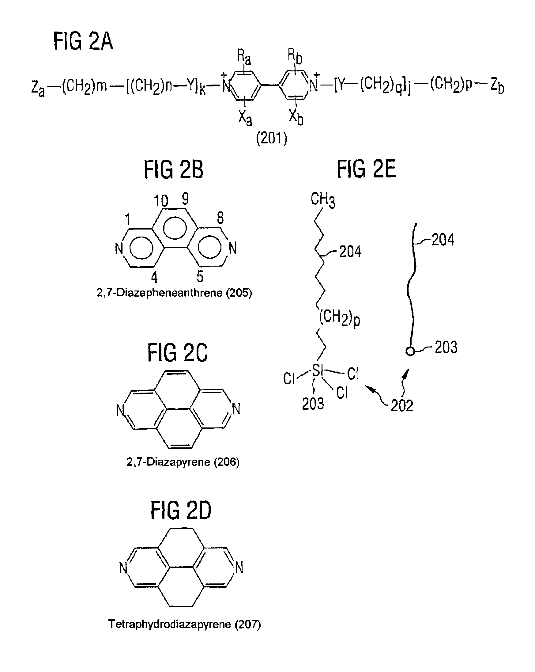
[0065]One preferred class of bispyridinium compounds is molecules with long-chain alkyl residues. These compounds have the advantage that they allow the formation of self-organizing layers of the redox-active molecules on the surface of the electrically conductive material. With compounds such as these, j and k in the formula (I) assume the values 0.
[0073]In one embodiment of the circuit element, a covalent bond of the redox-active compounds to the first and / or to the second conductive material is preferred since this makes it possible to ensure the orientation of the molecules and the (electrical) contact to the conductive materials.
[0086]In a refinement in which a large number of redox-active bispyridinium layers are used, an arrangement of such memory elements forms a memory matrix, i.e. it can be used as an electrical memory. One advantage of this refinement is the use of a molecular two-pole as a memory element, whereby the wiring complexity is reduced and the packing density is increased in comparison with conventional memory elements such as RAMs. The memory element according to the invention thus offers access to a highly integrated electrical memory. The memory element is preferably a permanent memory element, and the electrical memory which is based on a large number of memory elements is preferably a permanent memory. A permanent memory such as this may, for example, be used as a memory for graphics information, for example as a memory for on-chip video films.

Problems solved by technology

However, very low signals are observed during this switching process.
However, the two circuit elements which are known from [1] and [2] also have further disadvantages for widescale practical use.
Furthermore, the suitability of these Langmuir-Blodgett methods for the coating of surfaces of components such as silicon wafers, which are normally used for producing electrical components, is still uncertain.
Since nanotechnology is still in its infancy, it is questionable whether this system can be used for a practical application in the foreseeable future.

Method used


Image

  • Circuit element having a first layer composed of an electrically insulating substrate material, a method for producing a circuit element, bispyridinium compounds and their use in circuit elements
  • Circuit element having a first layer composed of an electrically insulating substrate material, a method for producing a circuit element, bispyridinium compounds and their use in circuit elements
  • Circuit element having a first layer composed of an electrically insulating substrate material, a method for producing a circuit element, bispyridinium compounds and their use in circuit elements

Examples


Embodiment Construction

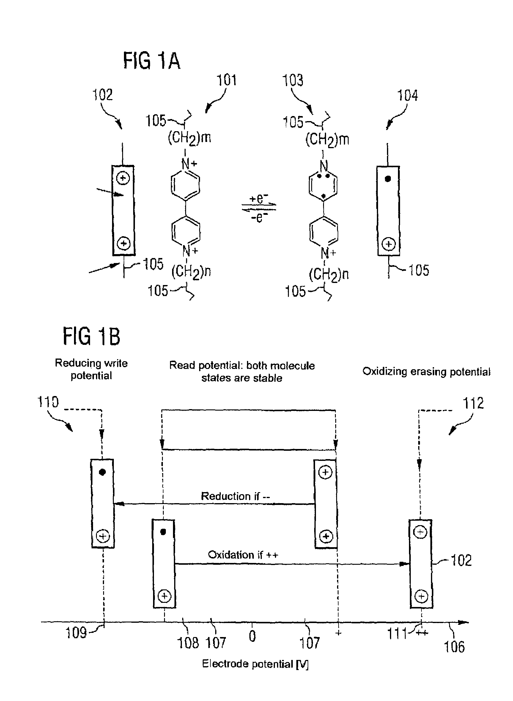
[0100]FIG. 1a shows a representation of a formula as well as a schematic illustration of the bispyridinium unit, on the basis of which the redox process, which takes place at the molecular level, of the bispyridinium unit (of the bispyridinium basic skeleton) is illustrated.

[0101]The double-positively charged cation 101, which has the reference number 102 in the schematic illustration, is the species which is not conductive below a predetermined reduction potential.

[0102]Above this predetermined reduction potential, the cation 101 represents an electron acceptor. After accepting an electron, the doubly-positively charged cation changes to the singly-positively charged radical cation 103 (104 in the schematic illustration). The free electron makes the radical cation electrically conductive. This state is below the oxidation potential of the radical cation 103. Above the oxidation potential, the radical cation in consequence represents an electron donator. The alkyl chains which are i...


PUM

PropertyMeasurementUnit
total lengthaaaaaaaaaa
electrically insulatingaaaaaaaaaa
electrically conductiveaaaaaaaaaa

Abstract

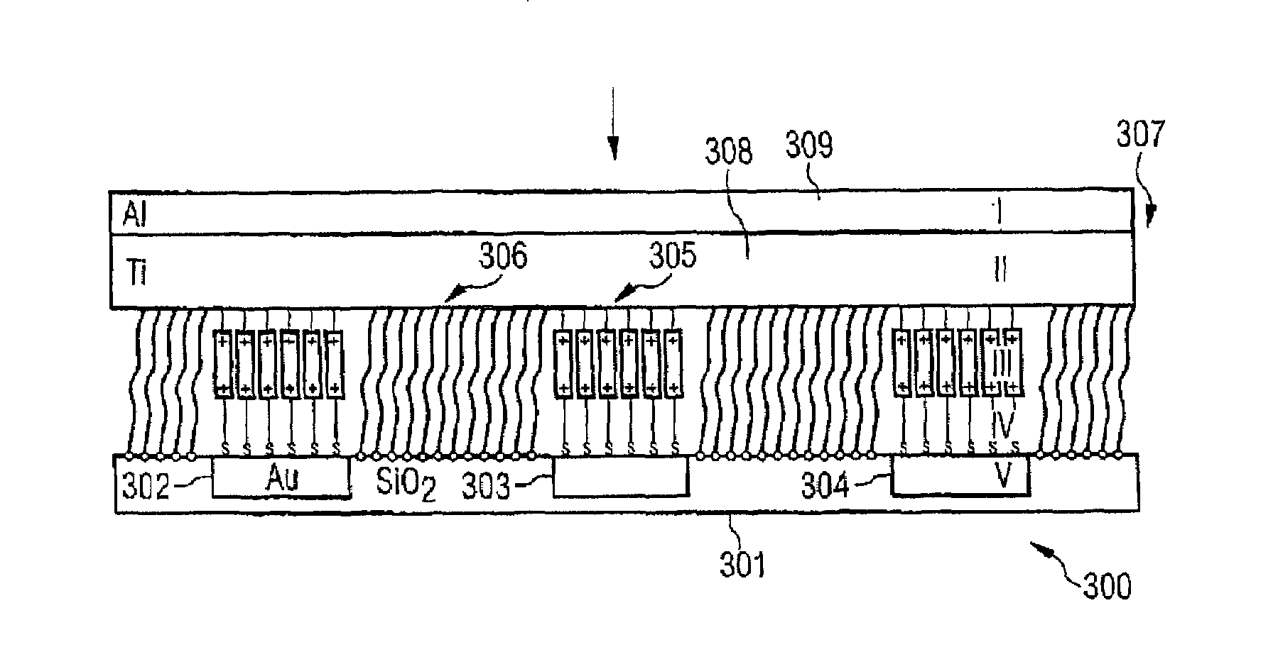
The circuit element has a first layer composed of an electrically insulating substrate material and a first electrically conductive material which is in the form of at least one discrete area such that it is embedded in the substrate material and / or is applied to the substrate material. Furthermore, it has a second layer having a second electrically conductive material, and a monomolecular layer composed of redox-active bispyridinium molecules, which is arranged between the first layer and the second layer. The bispyridinium molecules are immobilized on the electrically conductive material which is in the form of at least one discrete area, and make electrical contact with the second electrical material of the second layer. Furthermore, electrically inert molecules are immobilized on the first layer, which molecules form a matrix which surrounds the at least one discrete area with the monomolecular layer composed of bispyridinium molecules.

Description

BACKGROUND OF THE INVENTION[0001]The invention relates to a circuit element having a first layer composed of an electrically insulating substrate material, a method for a producing a circuit element, bispyridinium compounds and their use in circuit elements.[0002]1. Field of the Invention[0003]Conventional microelectronics, which are based on silicon components such as CMOS chips (CMOS: complementary metal-oxide-semiconductor), will also be reaching their limits as miniaturization progresses further. Molecular electronics are being discussed as one of the possible ways to reduce the size of components further.[0004]In addition to the general problem of developing circuit elements with the aid of molecular electronics, a further aspect under consideration in this context is the development of alternatives to the previous semiconductor memory elements such as DRAMs (Dynamic Random Access Memories), SRAMs (Static Random Access Memories) or Flash memories.[0005]2. Description of the Rel...

Claims


Application Information

Patent Timeline
Patent Type & Authority Patents(United States)
IPC IPC(8): H01L35/24C07D213/22G11C13/02H01L27/28H01L51/30
CPCB82Y10/00C07D213/22G11C13/0009G11C13/0014H01L51/0067H01L51/0072H01L51/0591H01L51/0595H01L27/28H10K19/00H10K85/654H10K85/6572H10K10/50H10K10/701
Inventor LUYKEN, R. JOHANNESSEITZ, MARKUSPREECE, JONWEBER, WERNERSCHMID, GUNTER
Owner QIMONDA
Learn More