Apparatus and method for manufacturing semiconductor grains

a technology of semiconductor grains and apparatuses, applied in the direction of manufacturing tools, sustainable manufacturing/processing, final product manufacturing, etc., can solve the problems of low productivity, and achieve the effect of preventing particle formation on the inner wall of the crucible and high conversion efficiency

Inactive Publication Date: 2006-02-21
KYOCERA CORP
View PDF13 Cites 17 Cited by
  • Summary
  • Abstract
  • Description
  • Claims
  • Application Information

AI Technical Summary

Benefits of technology

[0011]① As a crystal grain has a smaller granular diameter, the crystal quality of the grain is more improved, and in due course, the grain can become a single crystal. In other words, in a molten grain having a larger granular diameter, a number of cores as seed for crystallization are generated in the crystal. Therefore, without strictly controlling the temperature for growing crystal, the grain becomes polycrystalline.
[0013]From above, the granular diameter of a semiconductor grain used for a solar battery element has only to be reduced to a value not more than the thickness of a bulk crystal. With this preposition, if semiconductor grains respectively having uniform spherical shapes and excellent crystal quality can be inexpensively and conveniently manufactured without need of complicated steps, a reliable solar battery having an excellent quality can be provided at a low cost.
[0016]Further, according to a method for manufacturing semiconductor grains of the present invention, when the semiconductor molten solution is discharged out in the shape of drops from the nozzle member to allow to free-fall, a pressure is applied to the semiconductor molten solution in the crucible to discharge the same from the nozzle member in the shape of drops. Thereby, it becomes possible to manufacture semiconductor grains having uniform granular diameters and high crystallinity degree respectively.
[0019]As mentioned above, a method for manufacturing semiconductor grains according to the present invention includes steps of preliminarily mixing seeds acting as cores of crystallization into a semiconductor molten solution, then discharging out the semiconductor molten solution dropwise through the nozzle hole of the crucible to allow to free-fall, and cooling and solidifying the semiconductor molten solution during falling. The obtained semiconductor grains are of improved crystal quality and therefore they have an extremely high industrial value.
[0021]By such surface-treatment, particle formation on the inner wall of the crucible can be prevented. As a result, corrosion of the crucible is stopped and semiconductor grains having a carbon or other impurity concentration can be formed, so that a solar battery having a high converting efficiency can be manufactured.

Problems solved by technology

However, this method requires steps of grinding and classification, so that the manufacturing process becomes complicated and long, disadvantageously to lower the productivity.

Method used


Image

  • Apparatus and method for manufacturing semiconductor grains
  • Apparatus and method for manufacturing semiconductor grains
  • Apparatus and method for manufacturing semiconductor grains

Examples


first embodiment

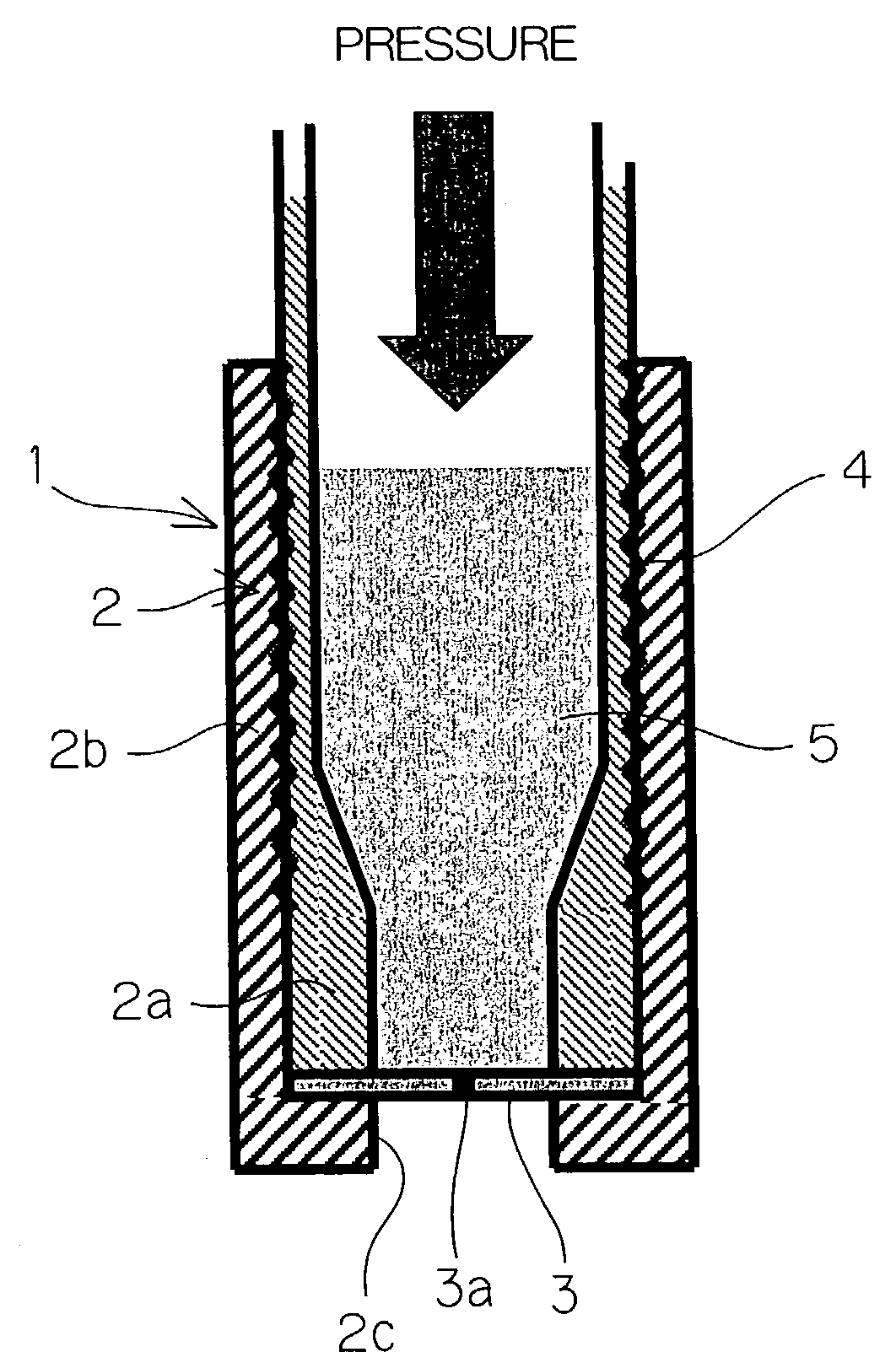
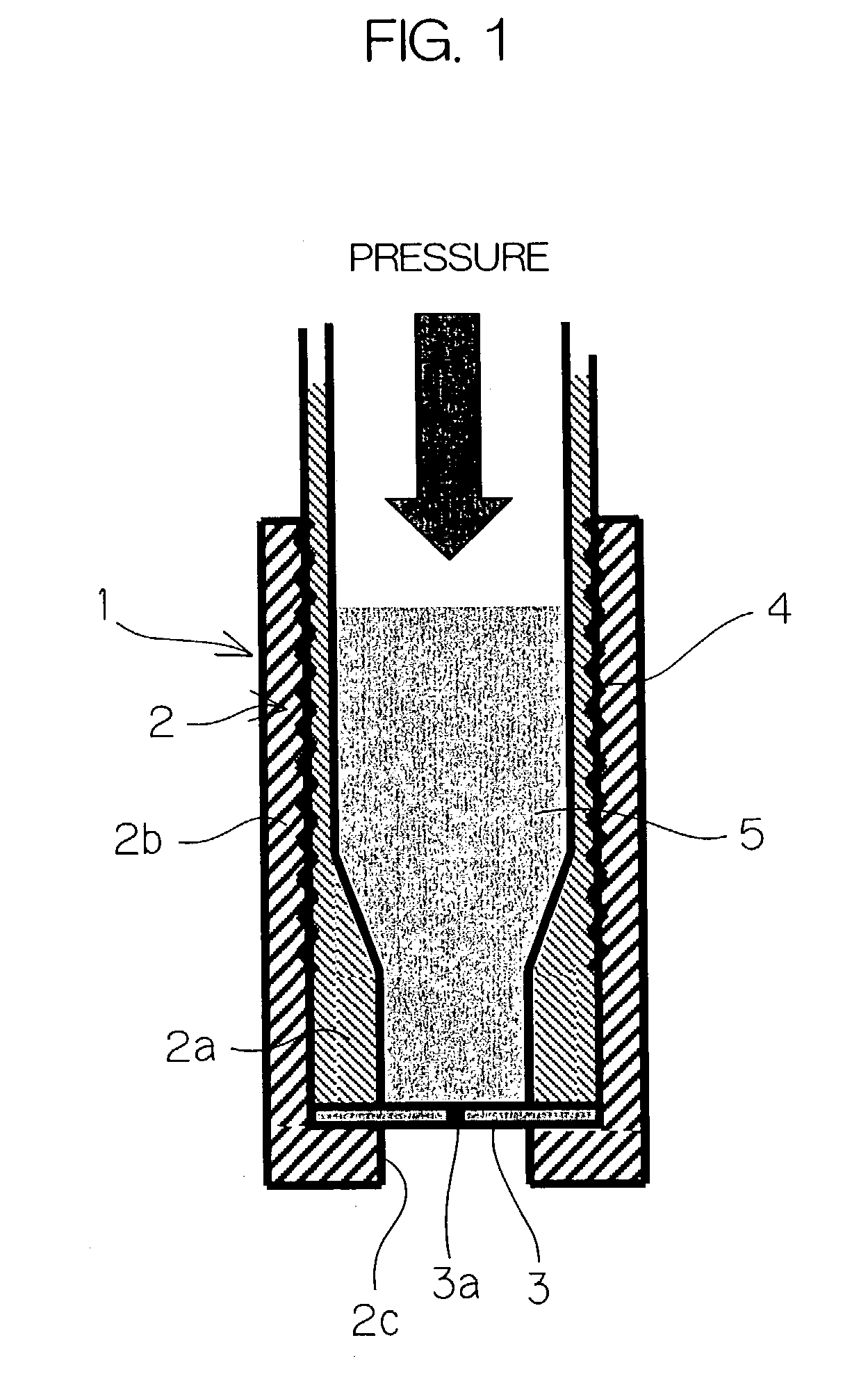
[0042]FIG. 1 is a view showing a crucible for manufacturing a semiconductor grains of an embodiment of the present invention. Numeral 1 indicates the whole of the crucible, and numeral 2 indicates a body member, numeral 3 indicating a nozzle member.

[0043]The crucible 1 comprises the cylindrical body member 2 and the disk-shaped nozzle member 3 fitted to the bottom portion of the body member 2.

[0044]The body member 2 comprises an inner wall member 2a having an inner wall hindering reaction with silicon and an outer wall member 2b disposed outside the inner wall member 2a. The outer wall member 2b is provided for reinforcing the body member 2. A screw 4 is threaded on each of the outside of the inner wall member 2a and the inside of the outer wall member 2b.

[0045]Each of the inner wall member 2a and the outer wall member 2b are formed of a sintered body compacted by casting, hot press or the like. Aluminum oxide, silicon carbide, graphite or the like is suitable for hindering reactio...

example 1

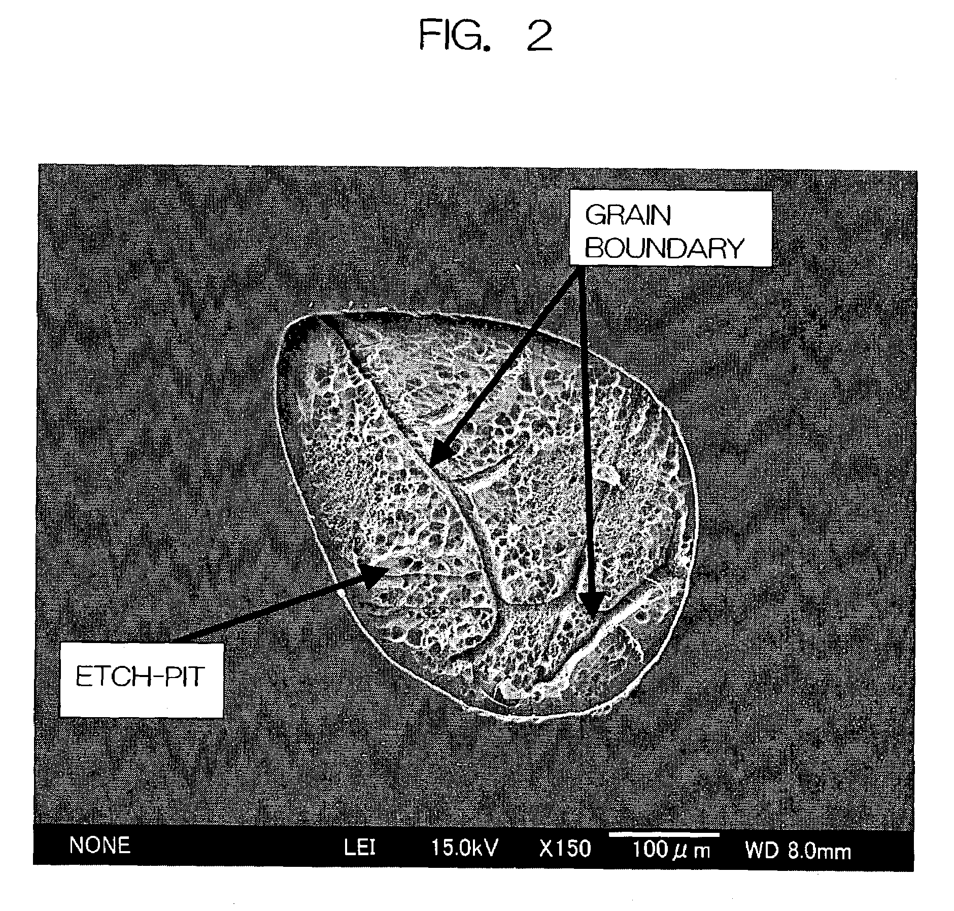
[0059]A nozzle members 3 having nozzle holes 3a of variety of diameters respectively worked by laser machining was manufactured to assemble a crucible. Then silicon in the crucible was melted and silicon grains were manufactured, and the diameters and crystal qualities of the obtained silicon grains were evaluated.

[0060]The test was carried out as follows.

[0061]18 grams of silicon material was filled into a crucible in an atmosphere of an inert gas such as Ar or He kept at a temperature of 1450° C. through a passage being similarly in an inert gas atmosphere, and melted. The crucible was formed of graphite (graphite DFP-2 manufactured by POCO Graphite, Inc. or the like) having dimensions of 19.0 mm φ in the inner diameter, 25.0 mm φ in the outer diameter and 143 mm in length. Variously changed gaseous pressures were applied to the sufficiently melted material to spray and discharge the whole amount of the molten material straight out through a nozzle hole. At this time, with the gas...

second embodiment

[0068]In this second embodiment, when silicon material is put into a crucible 1 and the whole of the silicon material is melted by the use of an induction heater or a resistance heater (not shown), grains acting as cores of crystallization are added to the silicon material.

[0069]These grains as cores of crystallization are preferably hard to react in the silicon molten solution. Grains of various kinds of materials can be used, if they do not change their shape or disperse as impurities to cause to lower the semiconductor quality. For example, aluminum oxide, silicon oxide, diamond, graphite or the like can be preferably used.

[0070]The silicon molten solution is pressed from above by argon gas or the like, for example, not more than 0.5 MPa to be extruded from the nozzle hole 3a of the nozzle member 3, so that the silicon molten solution is sprayed to make a number of drops. These drops of the silicon molten solution are allowed to free-fall. During falling, the drops are solidified...


PUM

PropertyMeasurementUnit
pressureaaaaaaaaaa
pressureaaaaaaaaaa
thicknessaaaaaaaaaa

Abstract

A crucible is formed of a cylindrical body member and a disk-shaped nozzle member fitted to the bottom portion of the body member, and the nozzle member is provided with a nozzle hole for discharging out a semiconductor molten solution dropwise therethrough. The semiconductor molten solution drops discharged out of the crucible through the nozzle hole are cooled and solidified during falling to become semiconductor grains. Silicon grains having high crystal quality can be manufactured at low cost.

Description

[0001]This application is based on applications Nos. 2001-325471, 2001-361551, 2001-392776 and 2002-020777 filed in Japan, the content of which is incorporated hereinto by reference.FIELD OF INVENTION[0002]The present invention relates to an apparatus and a method for manufacturing semiconductor grains.DESCRIPTION OF THE RELATED ART[0003]In developing next-generation solar batteries using silicon grains have been actively developed from the viewpoint of reducing the use amount of silicon and the manufacturing cost.[0004]A method for manufacturing silicon grains will be described in the following.[0005]As a material for manufacturing silicon grains, minute silicon grains obtained by grinding single crystal silicon material are used.[0006]The material silicon grains are classified by shape or weight, then heated by the use of infrared rays or a high frequency coil, and thereafter allowed to free-fall to be made into spherical shapes, whereby silicon grains are manufactured.[0007]Howev...

Claims


Application Information

Patent Timeline
Patent Type & Authority Patents(United States)
IPC IPC(8): B29B9/10C30B11/00C30B30/08H01L31/18
CPCC30B11/00C30B29/06C30B30/08H01L31/182H01L31/1804Y02E10/547Y02E10/546Y02P70/50
Inventor KITAHARA, NOBUYUKISUZUKI, TOSHIOSUDA, NOBORUSUGAWARA, SHINARIMUNE, HISAO
Owner KYOCERA CORP
Why Eureka
Try Eureka