

Apparatus and method for manufacturing semiconductor grains
a technology of semiconductor grains and equipment, applied in the direction of manufacturing tools, sustainable manufacturing/processing, final product manufacturing, etc., can solve the problem of low productivity
- Summary
- Abstract
- Description
- Claims
- Application Information
AI Technical Summary
Benefits of technology
Problems solved by technology
Method used
Image

Examples
second embodiment
[0068] Second Embodiment
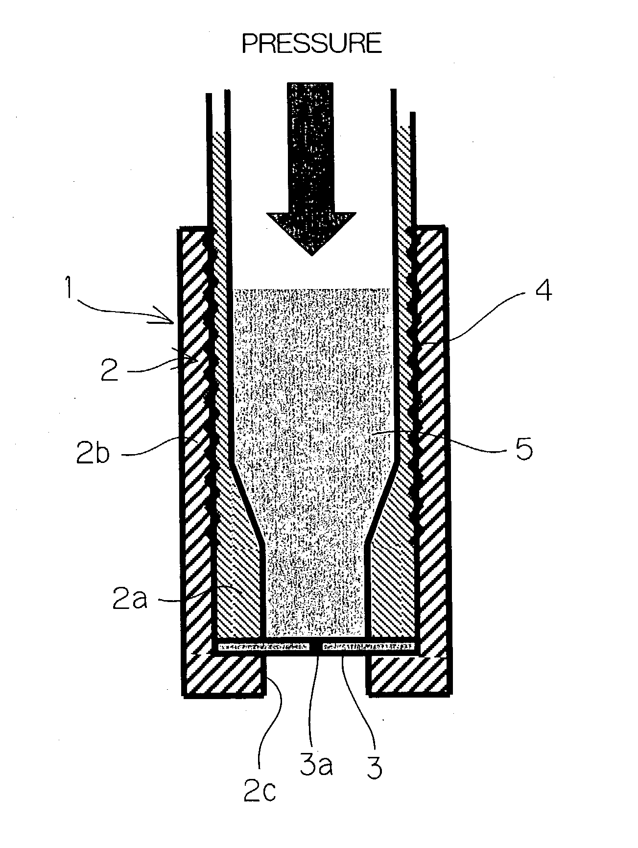
[0069] In this second embodiment, when silicon material is put into a crucible 1 and the whole of the silicon material is melted by the use of an induction heater or a resistance heater (not shown), grains acting as cores of crystallization are added to the silicon material.
[0070] These grains as cores of crystallization are preferably hard to react in the silicon molten solution. Grains of various kinds of materials can be used, if they do not change their shape or disperse as impurities to cause to lower the semiconductor quality. For example, aluminum oxide, silicon oxide, diamond, graphite or the like can be preferably used.
[0071] The silicon molten solution is pressed from above by argon gas or the like, for example, not more than 0.5 MPa to be extruded from the nozzle hole 3a of the nozzle member 3, so that the silicon molten solution is sprayed to make a number of drops. These drops of the silicon molten solution are allowed to free-fall. During fallin...
example 2
[0072] A crucible formed of graphite (graphite DFP-2 manufactured by POCO Graphite, Inc. or the like) having dimensions of 19.0 mm .phi. in the inner diameter, 25.0 mm .phi. in the outer diameter and 143 mm in length was used. The crucible had a nozzle member 3. A nozzle hole 3a of the nozzle member 3 is formed by laser machining.
[0073] The test was carried out as follows.
[0074] This crucible was set in a furnace capable of being kept at an atmosphere of an inert gas such as Ar or He, and the temperature was set at 1450.degree. C.
[0075] Grains acting as cores were weighed and added to the silicon material, and the mixture was uniformly dispersed in a container such as a polyethylene bag or the like. 18 grams of this silicon material containing the core grains was filled into the crucible kept at the temperature of 1450.degree. C. through a passage similarly kept in an atmosphere of an inert gas and melted.
[0076] Gaseous pressure of 0.15 MPa was applied to the sufficiently melted sil...
example 2-1
[0078] 0.02 grams of silicon carbide grains (2-3 .mu.m) as cores were weighed and added to silicon material, and the mixture was uniformly dispersed in a container such as a polyethylene bag or the like. Thereafter, the silicon material is sprayed under the above-mentioned condition.
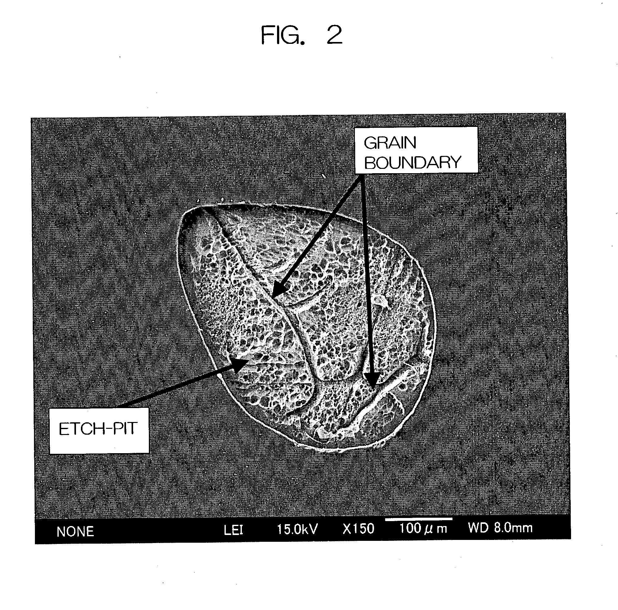
[0079] The obtained silicon grains were classified by shape. The result was that the grains were classified into {circle over (1)} tear-shaped grains {circle over (2)} diamond-shaped grains and {circle over (3)} spherical grains, and the constitutional ratio was 2:7:1.
[0080] The sectional surfaces of the grains of each of the abovementioned shapes were subjected to SEM (Scanning Electron Microscope) observation, and the result is shown in FIGS. 2 to 4.
[0081] The SEM observation was carried out by embedding each silicon grain into a resin and grinding and mirror-finishing its sectional surface, thereafter sufficiently etching the same with a mixed acid of hydrofluoric acid, nitric acid and acetic acid, an...
PUM
| Property | Measurement | Unit |
|---|---|---|
| diameter | aaaaa | aaaaa |
| diameter | aaaaa | aaaaa |
| pressure | aaaaa | aaaaa |
Abstract
Description
Claims
Application Information