Method and apparatus for locating/sizing contaminants on a polished planar surface of a dielectric or semiconductor material

a dielectric or semiconductor material, highly polished technology, applied in the direction of color/spectral properties measurement, instruments, material analysis, etc., can solve the problems of existing wafer scanning tools, time-consuming searching for sub-micron contaminants, and non-functional chips, so as to minimize the specular reflection of incident light, maximize the capture of scattered light, and the effect of high numerical apertur

Active Publication Date: 2006-02-21
SYNETICS SOLUTIONS +2
View PDF16 Cites 74 Cited by
  • Summary
  • Abstract
  • Description
  • Claims
  • Application Information

AI Technical Summary

Benefits of technology

[0010]The present invention is not really concerned with classifying the surface contaminants as particles, scratches, crystal-originated pits (COPs), other pits, dimples, etc. or identifying their material which may require specific (and possibly a multiplicity of) light sources and detector orientations, polarizations, etc. as suggested in the prior art. Rather, the present invention is aimed at describing a comparatively simple, compact and portable apparatus and method to locate / size surface contaminants on a bare dielectric or semiconductor material.
[0014]The high numerical aperture scattered light collector maximizes the capture of the scattered light from a contaminant. This coupled with illumination at Brewster's angle, which minimizes specular reflection of incident light from the wafer surface, maximizes the signal-to-noise ratio. This combination of items has not been exploited in the prior art dealing with wafer scanning apparatuses. The prime sources of noise in the system are scatter from sub-micron surface roughness (haze) on the wafer surface and detector dark current. The combination of these is small and relatively constant.

Problems solved by technology

Particle deposition on a wafer is a major cause of non-functional chips.
A particle on a wafer surface can cause (1) an electrical “open” or “shorted” circuit, depending on its location relative to the electrical conductors or (2) damage to the chip as a result of chemical reactions surrounding the particle.
Because of the high magnification of this instrument, searching for sub-micron contaminants can be time consuming.
Chief among the drawbacks is the fact that existing wafer scanning tools, based on the prior art, are located and used off-the-process line due primarily to size, weight, and lack of portability (sensitivity to movement).
The cumulative transport time delays identifying and correcting contamination problems in the manufacturing equipment and decreases production time.
Other perceived drawbacks to existing wafer scanning tools include complexity (number of parts), large footprint, and high cost.

Method used


Image

  • Method and apparatus for locating/sizing contaminants on a polished planar surface of a dielectric or semiconductor material
  • Method and apparatus for locating/sizing contaminants on a polished planar surface of a dielectric or semiconductor material
  • Method and apparatus for locating/sizing contaminants on a polished planar surface of a dielectric or semiconductor material

Examples


second embodiment

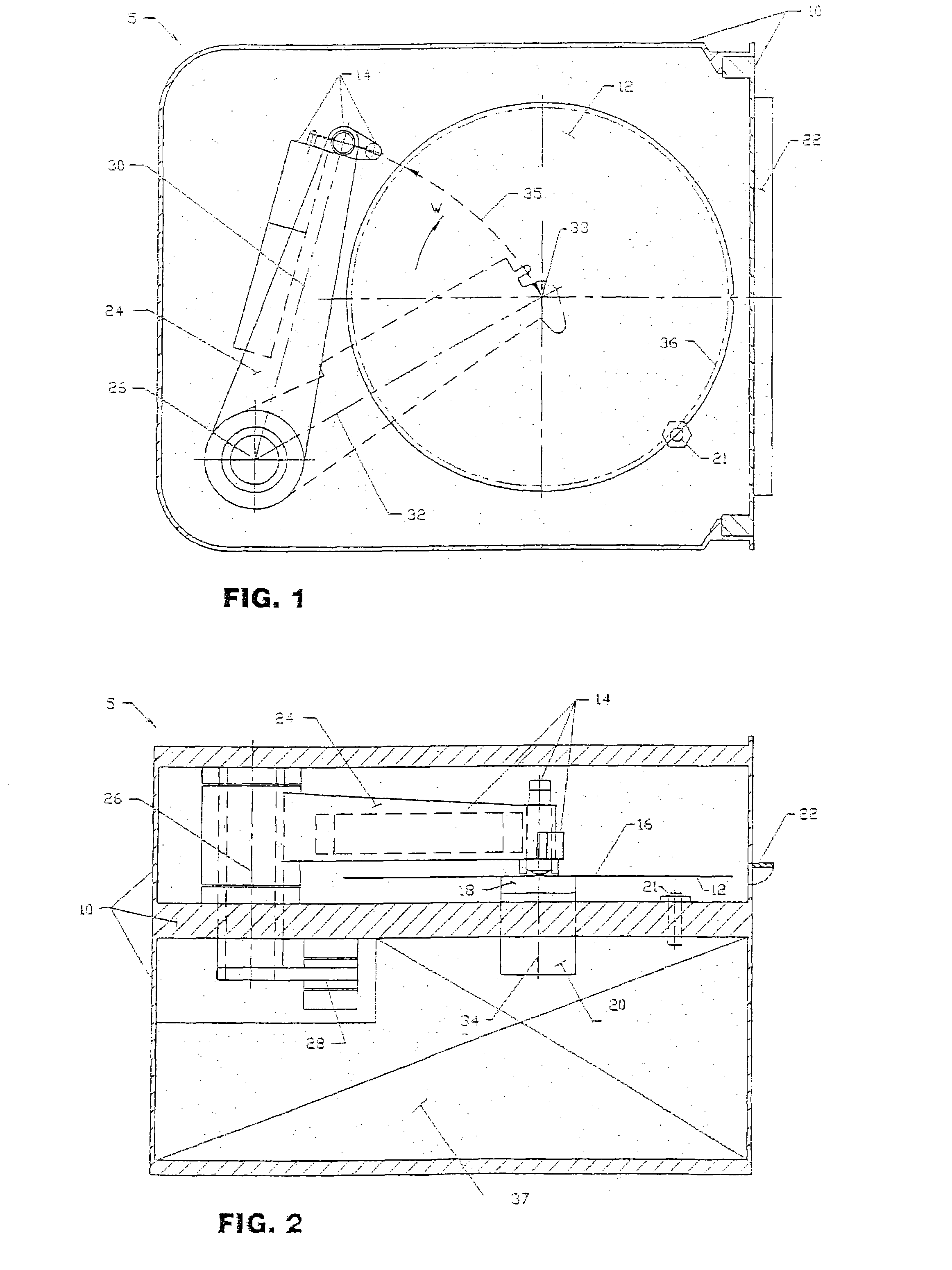
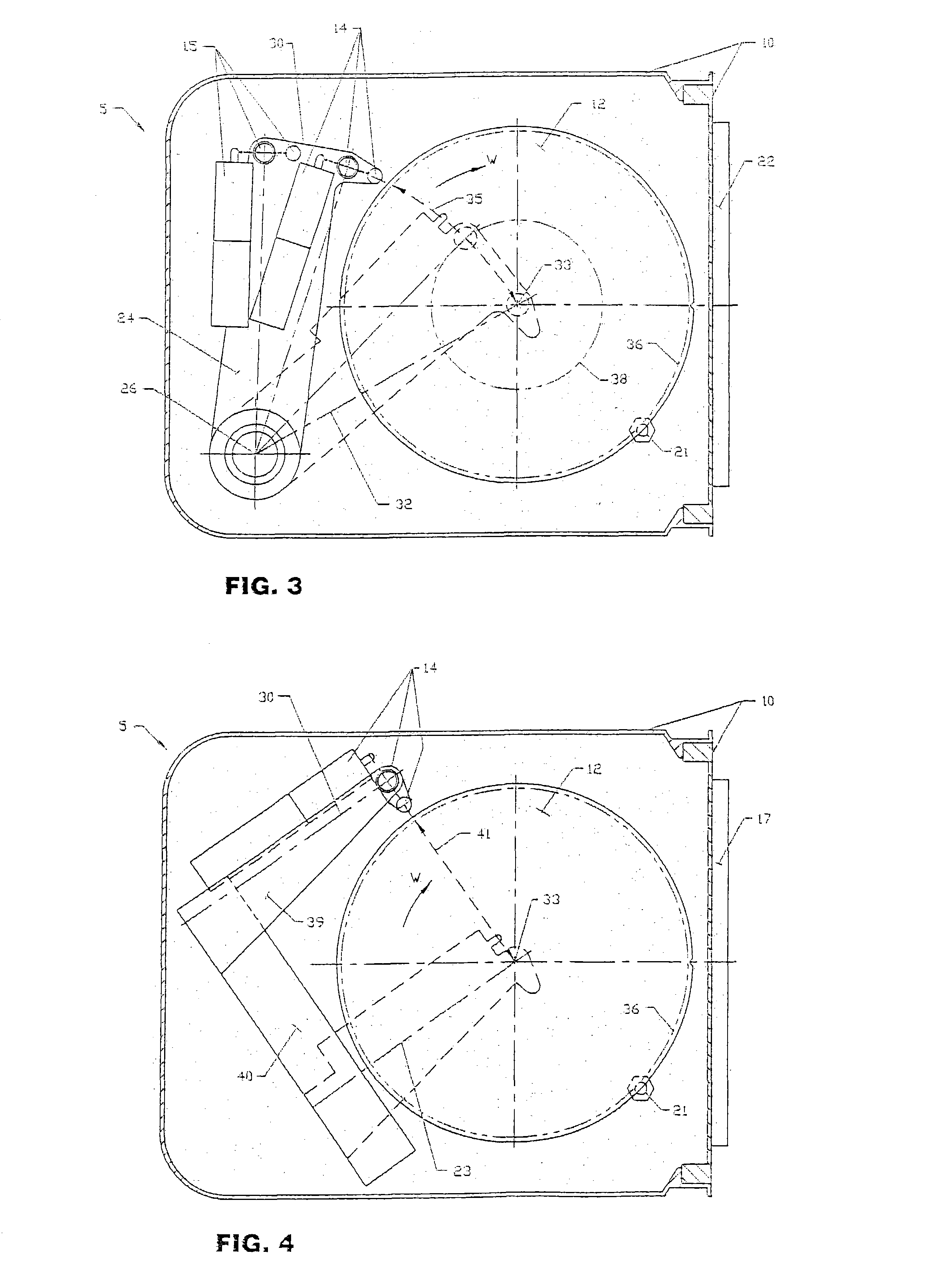
[0036]FIG. 3 illustrates scanning module 5 in which the time to scan a wafer is halved by modifying pivot arm 24 to accommodate a second instrument group 15, identical to and spaced from instrument group 14 by a distance approximately equal to half the wafer radius along arc 35. All other elements of scanning module 5 are otherwise unchanged. Instrument group 14 thus scans from a new start scan circle 38 to stop scan point 33 while instrument group 15 simultaneously scans from start scan circle 36 to a stop scan circle that is essentially the same as start scan circle 38 for instrument group 14 (in practice there is a small overlap of these start and stop scan circles). Start scan circle 38 has half the radius of start scan circle 36.

third embodiment

[0037]scanning module 5 is illustrated in FIG. 4 wherein pivoting arm 24 is replaced by a cantilever arm 39 attached to a linear stage 40 to move instrument group 14 so that its projected laser beam illuminated spot follows a linear path 41 on wafer top surface 16. All other elements of scanning module 5 are otherwise unchanged.

[0038]It follows that the dual instrument group concept of FIG. 3, used to halve the scan time, can be extrapolated to include more than two instrument groups disposed on a suitable pivot arm (ala FIG. 3) or cantilever arm (ala FIG. 4) where the scan time reduction factor is the member of instrument groups employed.

[0039]Irrespective of the scanning module 5 internal configuration the overall compact and portable system data processing electronics / computers, power supplies / distribution, vacuum source, and touch screen control / display are located outside of scanning module 5 as conceptually illustrated in FIG. 5. Therein the overall system is comprised of scan...

first embodiment

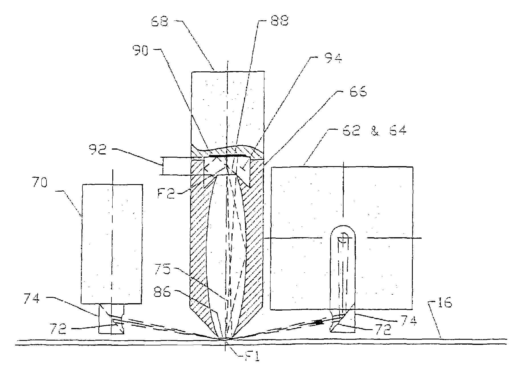
[0050]FIGS. 10A and 10B in conjunction with FIGS. 1 through 4, presents top and front views (showing component relative size proportions) of instrument group 14 positioned at a constant distance just above wafer top surface 16 and configured according to scanning module 5. Instrument group 14 is comprised of a laser 62 (in the ≦470 nm preferred wavelength range), laser beam conditioning optics 64, scattered light collector 66 (a highly elongate ellipsoidal reflector), a scattered light detector 68, and the optional reflected light beam dump / CCD camera (or other detector) 70.

[0051]The laser beam conditioning optics 64 include an electronically controlled beam shutter and produce a diffraction limited beam with a circular cross-section, a symmetrical Gaussian irradiance distribution about the optical axis, and finely focused to a circular point centered on the optical axis of the beam. The focal point on the laser beam optical axis is permanently positioned to be coincidental with the...


PUM

PropertyMeasurementUnit
diameteraaaaaaaaaa
diameteraaaaaaaaaa
single wavelengthaaaaaaaaaa

Abstract

To locate / size contaminants at the surface of a dielectric or semiconductor material, a P-polarized beam of light from a monochromatic solid-state source is disposed specifically at Brewster's angle and focused to form an illuminated quasi-elliptical spot on the surface that produces effectively no reflected or scattered light from the surface. The spot is scanned over the entire surface so as to assure multiple passes of any contaminant through the spot. On each pass through the spot a contaminant will produce scattered light. A novel high numerical aperture reflective or refractive system is disposed above the surface to always view the spot and to collect / redirect the bulk of the contaminant scattered light to a detector. Illumination at Brewster's angle combined with the high numerical aperture scattered light collector / redirector maximizes the signal-to-noise ratio from the detector. These core components are packaged with support subsystems as a uniquely compact and portable apparatus.

Description

BACKGROUND OF THE INVENTION[0001]This invention relates generally to a method for inspecting a bare highly polished planar surface of a dielectric or semiconductor material for contaminants thereon.[0002]In manufacturing semiconductor devices, multiple identical microcircuits are formed on bare highly polished planar semiconductor (silicon) wafers using a variety of sophisticated automated equipment (tools, machines). Critically essential to this manufacturing process is a requirement that the wafers are free of contaminants on or at their surface (e.g.: particles, scratches, etc.). To this end, the semiconductor manufacturing equipment is specifically designed, tested, and assembled in clean rooms prior to shipment to minimize all sources that could contaminate a wafer surface during use of the equipment. Additionally, upon arrival at the semiconductor fabrication facility the equipment is installed in large clean room areas that are also stringently controlled to minimize the poss...

Claims


Application Information

Patent Timeline
Patent Type & Authority Patents(United States)
IPC IPC(8): G01N21/00G01N21/21G01N21/27G01N21/47G01N21/94G01N21/95
CPCG01N21/21G01N21/278G01N21/9501G01N21/94G01N21/47
Inventor MACGIBBON, BRUCEADAMSKI, DONALD F.STEVENS, TODD
Owner SYNETICS SOLUTIONS
Why Eureka
Try Eureka