

Memory cell architecture
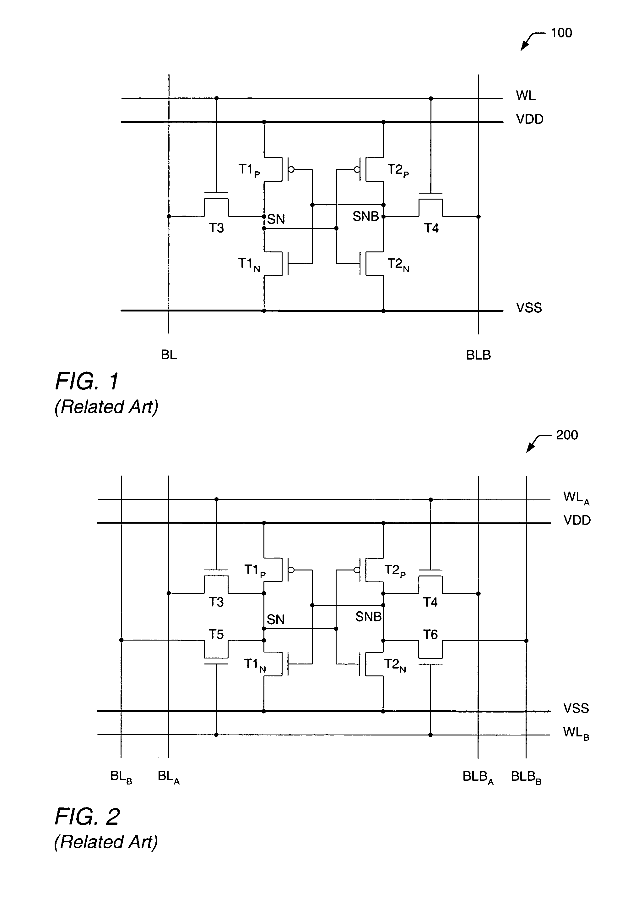
a memory cell and memory technology, applied in static storage, digital storage, instruments, etc., can solve the problems of capacitive memory cells not maintaining their contents, ram storage is generally volatile, and leakage currents within semiconductor memory are unavoidable, so as to reduce intrinsic and cross-coupling bitline capacitance, cross-coupling intrinsic bitline capacitance may be reduced
- Summary
- Abstract
- Description
- Claims
- Application Information
AI Technical Summary
Benefits of technology
Problems solved by technology
Method used
Image

Examples
Embodiment Construction
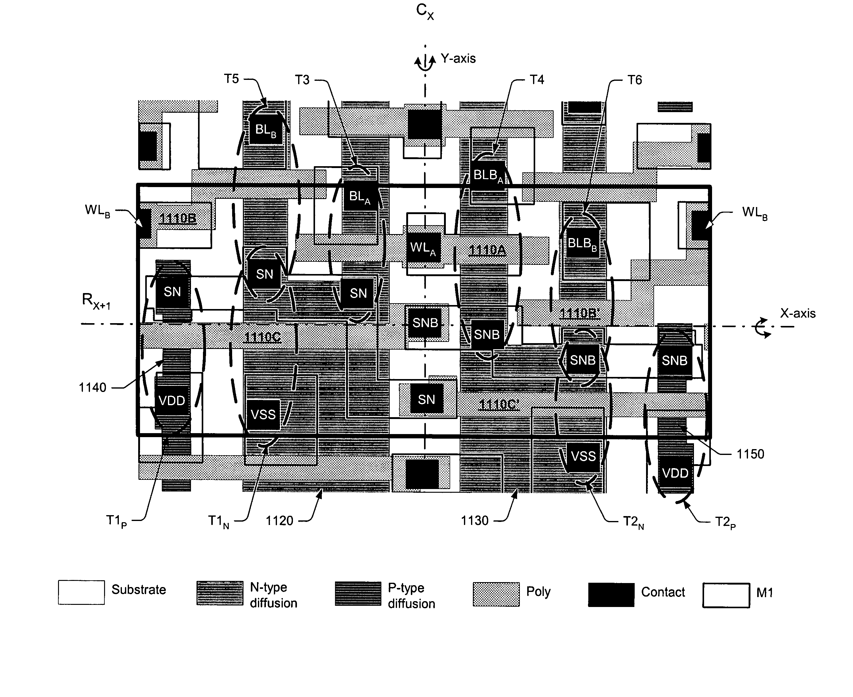
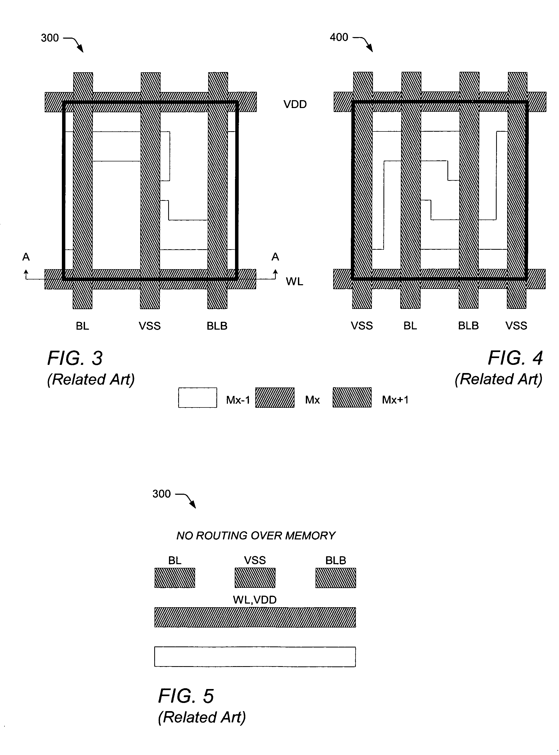
[0050]FIGS. 3–5 illustrate exemplary embodiments of a cell architecture that may be used to form a single-port SRAM cell, such as memory cell 100 of FIG. 1. FIGS. 3 and 4 present top-down views of cell architectures 300 and 400, respectively. FIG. 5 presents a cross-sectional view along line AA of cell architecture 300. Though the architecture of only one memory cell is illustrated in FIGS. 3–5, and later in FIGS. 6–9, one of ordinary skill in the art would understand how the architecture could be applied to an array of memory cells.
[0051]In most SRAM architectures, including those illustrated in FIGS. 3–5, the bitlines and wordlines of the memory cell run orthogonal to one another on separate metallization layers. Therefore, at least two metallization layers are needed to form an SRAM cell. In some cases, more than two metallization layers may be used in an effort to increase cell density by decreasing the cell aspect ratio. In general, the term “aspect ratio” is used herein to des...
PUM
 Abstract
Description
Claims
Application Information