Method for forming image on object surface including circuit substrate

a technology of image and object surface, applied in the direction of resistive material coating, conductive material electric discharge removal, nuclear engineering, etc., can solve the problems of time and cost, large cost and time required to form the photomask, and the use of the photomask for exposur

Inactive Publication Date: 2006-03-07
DAIKEN CHEM
View PDF7 Cites 5 Cited by
  • Summary
  • Abstract
  • Description
  • Claims
  • Application Information

AI Technical Summary

Benefits of technology

[0029]Tenth form of the present invention is the method according to said eighth form, wherein said unsintered image pattern i

Problems solved by technology

However, the weakest point of this circuit substrate is that the photomask is used for exposure.
The first weak point of photomask utilization is that the great cost and time are required to form the photomask.
Therefore, time and cost are necessary by all means, because a few days are needed to make a piece of work mask.
The second weak point of photomask utilization is that there is a limitation in precision of the pattern.
The third weak point of photomask utilization is that the latent image cannot be formed according to the fineness of dimension of a photomask because the ultraviolet radiation is diffracted through the photomask.
It is better that photomask is adhe

Method used


Image

  • Method for forming image on object surface including circuit substrate
  • Method for forming image on object surface including circuit substrate
  • Method for forming image on object surface including circuit substrate

Examples


first embodiment

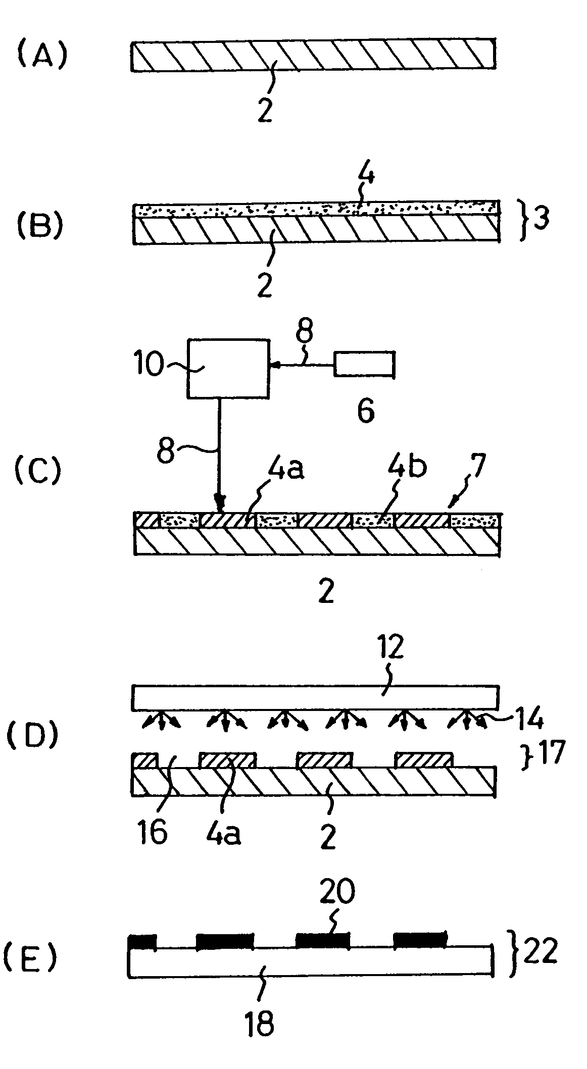
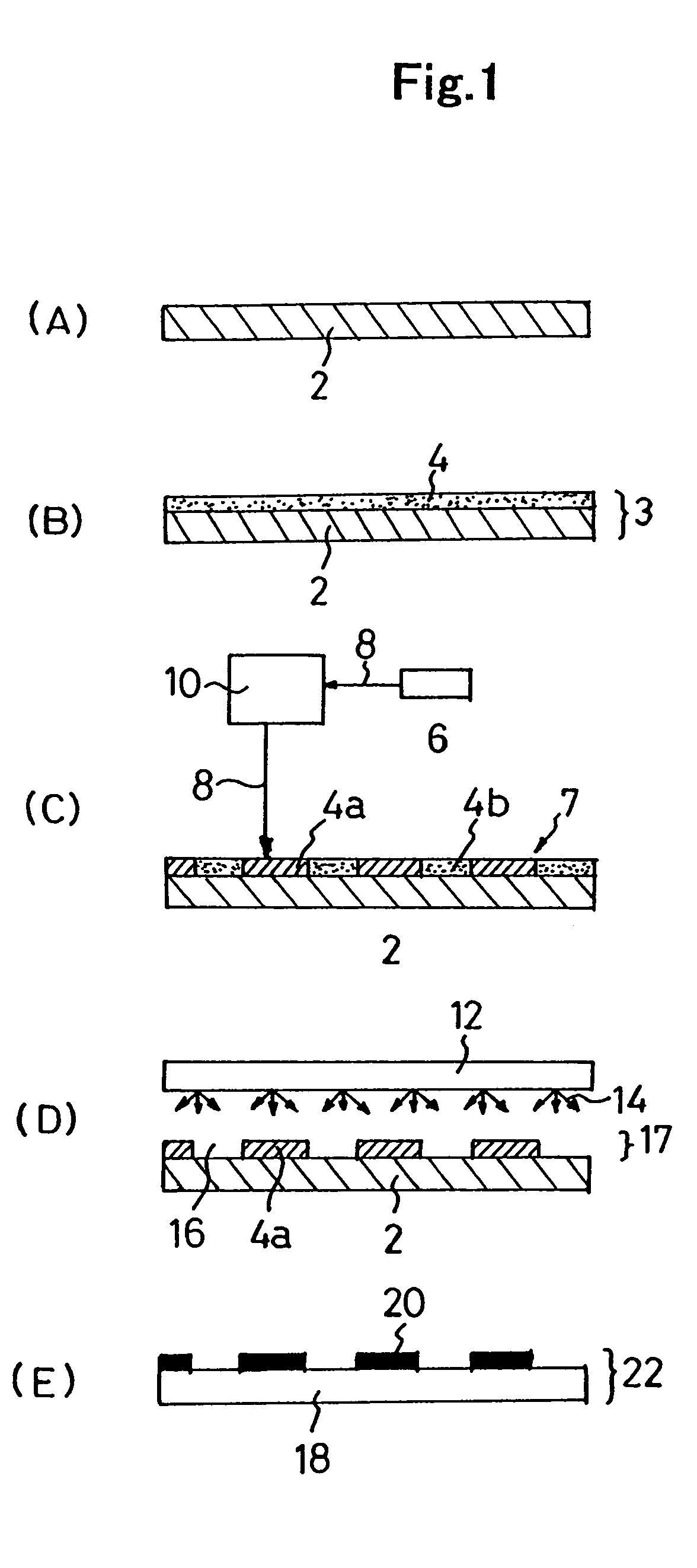
[0043]FIG. 1 is a manufacturing process diagram of one layer circuit substrate of the present invention. In the process of (A), the greensheet 2 which becomes a board of circuit substrate is arranged in a predetermined location. First, ceramic powder which becomes a base agent of greensheet 2 is prepared. Various materials are employed as the ceramic powder. For example, the mixture of borosilicate glass powder consisting of CaO.Al2O3.B2O3.SiO2 system and alumina powder with a weight ratio of 60:40 may be used.

[0044]A slurry is prepared by mixing the ceramics powder, organic solvent, organic binder and plasticizer, and the slurry is formed to a sheet of 1 to 300 μm in thickness by doctor blade method, and then a raw greentape is made by winding the sheet. The greensheet 2 is formed by cutting the greentape with a predetermined length.

[0045]In the process of (B), photosensitive paste layer 4 made by applying photosensitive paste to the surface of the greensheet 2 and then the unexpos...

second embodiment

[0070]FIG. 3 is the manufacturing process diagram of multilayer circuit substrate in second embodiment of the present invention. In this embodiment, a plurality of greensheet 2 formed unsintered circuit pattern are laminated, and then the multilayer circuit substrate is formed by sintering it. Codes repeated in FIG. 1 represent the same members.

[0071]In the process of (A), greensheet 2 having through hole 5 is arranged in an predetermined position. In the process of (B), photosensitive paste is made from mixture of photoresist and circuit materials, and the paste is applied to the surface of the greensheet 2 to form the photosensitive paste layer 4. The photosensitive paste is also filled in the through hole 5.

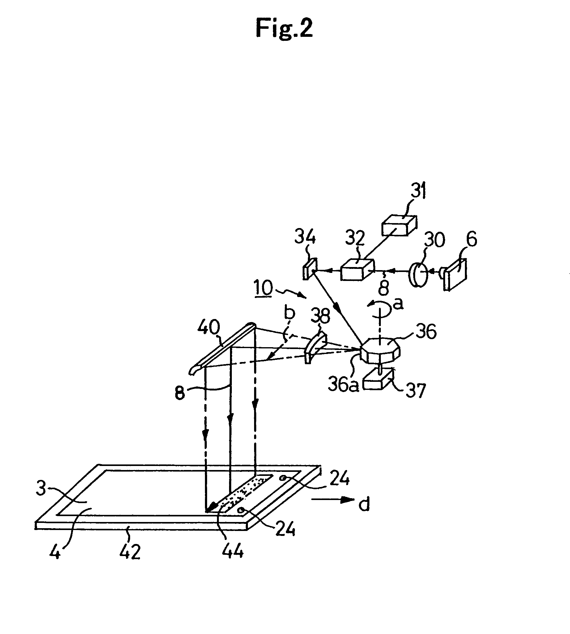
[0072]In the process of (C), said laser beam 8 is emitted from the laser light source 6, and the laser beam 8 is converted to dot pattern (on-off pattern) with the laser plotting device 10 and said beam scans under control of the device to form an arbitrary circuit pattern on ...


PUM

PropertyMeasurementUnit
Densityaaaaaaaaaa
Thermal resistanceaaaaaaaaaa
Photosensitivityaaaaaaaaaa

Abstract

By using a novel method, the exposure time of the photosensitive paste layer is reduced and the exposure fineness of the layer is improved, thereby developing a highly fine circuit substrate of high density having a thermal resistance at a reasonable cost. A circuit substrate is manufactured as follows. A photosensitive paste containing photoresist and a circuit material is applied onto a substrate surface so as to form a photosensitive paste layer (4). This photosensitive paste layer (4) is plotted by a laser beam (8) so as to form a plotted area (7). The photosensitive paste layer (4) is developed and an exposed area (4a) or an unexposed area (4b) is removed so as to form a circuit pattern (17). This circuit pattern (17) is sintered to form a circuit pattern (20) composed of the circuit material. It is possible to form a highly fine circuit pattern of high density by laser beam plotting. Moreover, when a greensheet (2) is used as the substrate, it is possible to form a ceramic substrate (18) having a thermal resistance by sintering. Furthermore, by using this method, it is possible to form an arbitrary image on an arbitrary object.

Description

TECHNICAL FIELD[0001]The present invention relates to a method for forming image on an object surface including circuit substrate, and more specifically relates to the method for forming image on the object surface comprised by the steps of scanning a laser beam to irradiate for a photosensitive paste layer which consists of a mixture of colorant materials and photoresist, forming a plotting area consisted of highly fine image patterns, and developing the photosensitive paste layer to form the highly fine image pattern.BACKGROUND ART[0002]As the object having image pattern, there are circuit substrate, mug, craftwork and so on. The circuit substrate is an object which is formed a circuit pattern on a surface thereof the mug is an object having a decoration image on outer circumferential surface of the cup which is made from ceramics, and many of craftworks are the objects formed an industrial art decoration image on the surface of industrial art articles. Since highly fine and densi...

Claims


Application Information

Patent Timeline
IPC IPC(8): G03F7/00H05K1/09H05K3/02H05K3/46
CPCH05K3/02H05K1/092Y10S430/146H05K2203/0514H05K2203/107H05K3/4611H05K3/08
Inventor KATO, MASATOSHIHARADA, AKIO
Owner DAIKEN CHEM
Why Eureka
Try Eureka