Massively parallel interface for electronic circuit

a technology of electronic circuits and interfaces, applied in the direction of individual semiconductor device testing, electrical apparatus contruction details, instruments, etc., can solve the problems of limited number of parallel testing on the wafer level, plagued wafer-level burn-in, limited pin count devices, etc., to reduce assembly manufacturing costs and manufacturing time, the effect of high speed

Inactive Publication Date: 2006-03-07
ADVANTEST SINGAPORE PTE LTD
View PDF227 Cites 59 Cited by
  • Summary
  • Abstract
  • Description
  • Claims
  • Application Information

AI Technical Summary

Benefits of technology

[0030]Several embodiments of massively parallel interface integrated circuit test assemblies are disclosed, which use one or more substrates to establish connections between one or more integrated circuits on a semiconductor wafer, and use one or more test modules which are electrically connected to the integrated circuits on the semiconductor wafer through the substrates. One or more layers on the intermediate substrates preferably include MEMS and / or thin-film fabricated spring probes. The massively parallel interface assemblies provide tight pad pitch and compliance, and preferably enable the parallel testing or burn-in of multiple ICs. In some preferred embodiments, the massively parallel interface assembly structures include separable standard electrical connector components, which reduces assembly manufacturing cost and manufacturing time. These massively parallel interface structures and assemblies enable high speed testing in wafer form, and allow test electronics to be located in close proximity to the wafer. Preferred embodiments of the massively parallel interface assemblies provide thermal expansion matching to the wafer under test, and provide a thermal path for system electronic. Alternate massively parallel interface structures provide massively parallel connection interfaces, which may be used in a wide variety of circuitry, such as for interconnecting computers in a network, or for interconnecting other electronic circuitry.

Problems solved by technology

Parallel testing on the wafer level has been limited in number and has so far been limited to low pin count devices, due to the difficulty in managing the large number of interconnects, and the limited amount of electronics which can conventionally be placed close to a wafer under test.
However, wafer-level burn-in is plagued with multiple problems, such as thermal expansion mismatch between the connector and the silicon wafer under test.
However, semiconductor test costs have increased on a cost per unit area of silicon basis.
Therefore, semiconductor test costs have increased disproportionately over time, to become a greater percentage of the total manufacturing cost for each integrated circuit device.
Furthermore, advances in chip scale packaging (CSP) and other forms of small footprint packages have often made traditional packaged IC handlers obsolete for testing and burn-in.
However, tungsten needle probe technology is not able to meet the interconnect requirements of advanced semiconductors having higher pin counts, smaller pad pitches, and higher clock frequencies.
While emerging technologies have provided spring probes for different probing applications, most probes have inherent limitations, such as limited pitch, limited pin count, varying levels of flexibility, limited probe tip geometries, limitations of materials, and high costs of fabrication.
While the contact tip structures disclosed by B. Eldridge et al. provide resilient contact structures, the structures are each individually mounted onto bond pads on semiconductor dies, requiring complex and costly fabrication.
As well, the contact tip structures are fabricated from wire, which often limits the resulting geometry for the tips of the contacts.
Furthermore, such contact tip structures have not been able to meet the needs of small pitch applications (e.g. typically on the order of 50 μm spacing for a peripheral probe card, or on the order of 75 μm spacing for an area array).
The spring contact is made of an elastic material and the free portion compliantly contacts a second contact pad, thereby contacting the two contact pads.” While the photolithography patterned springs, as disclosed by Smith et al., are capable of satisfying many IC probing needs, the springs are small, and provide little vertical compliance to handle the planarity compliance needed in the reliable operation of many current IC prober systems.

Method used


Image

  • Massively parallel interface for electronic circuit
  • Massively parallel interface for electronic circuit
  • Massively parallel interface for electronic circuit

Examples


Embodiment Construction

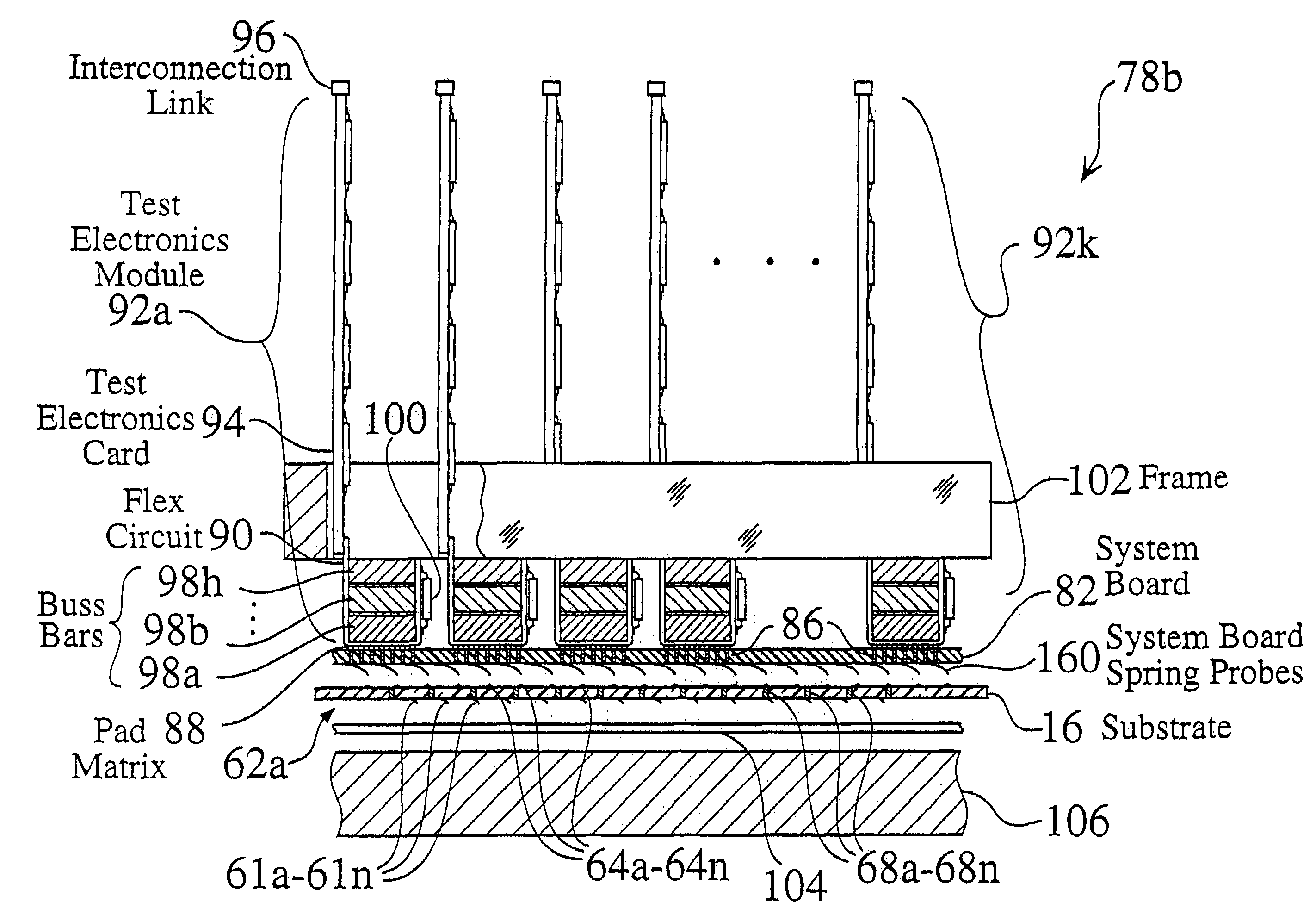
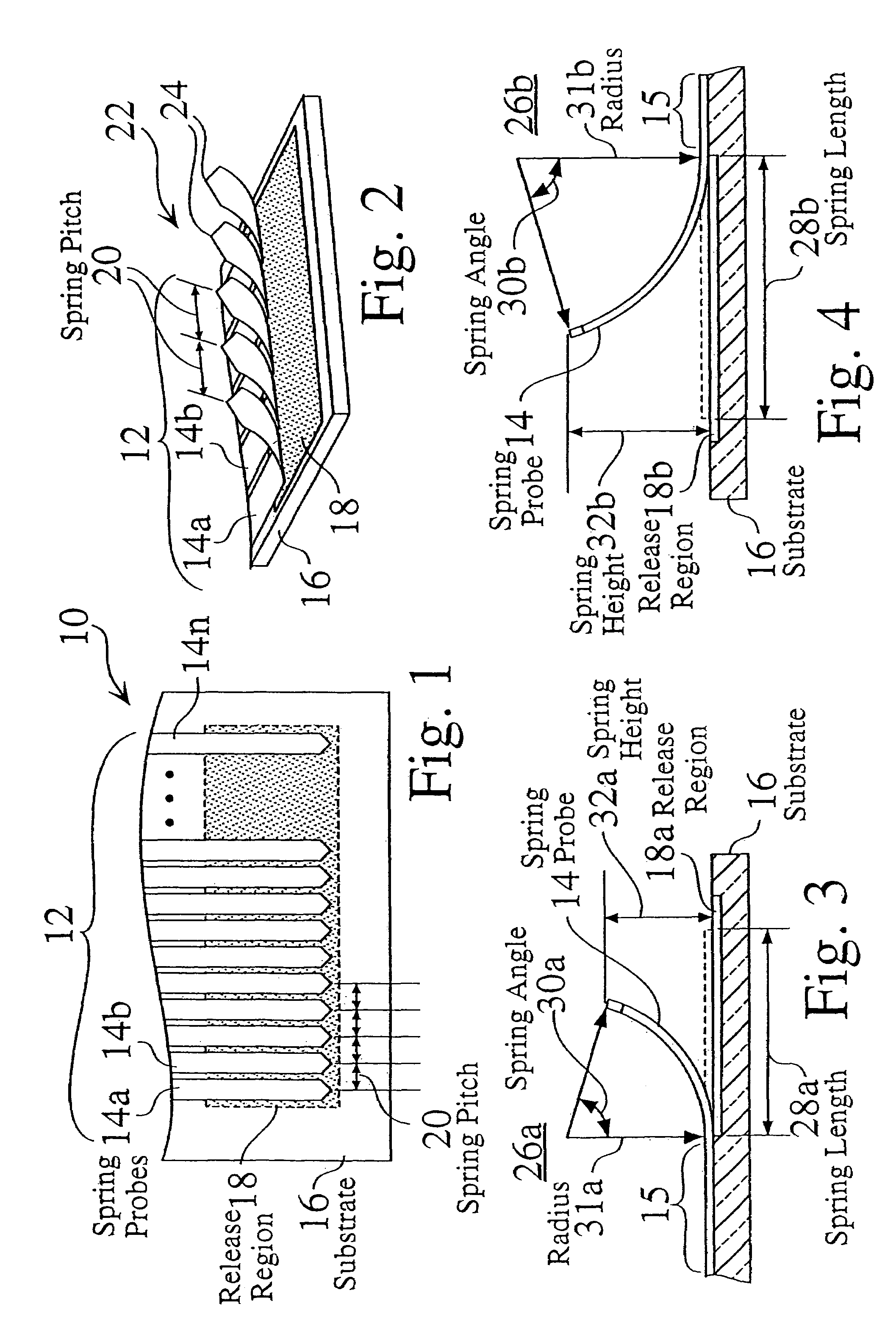
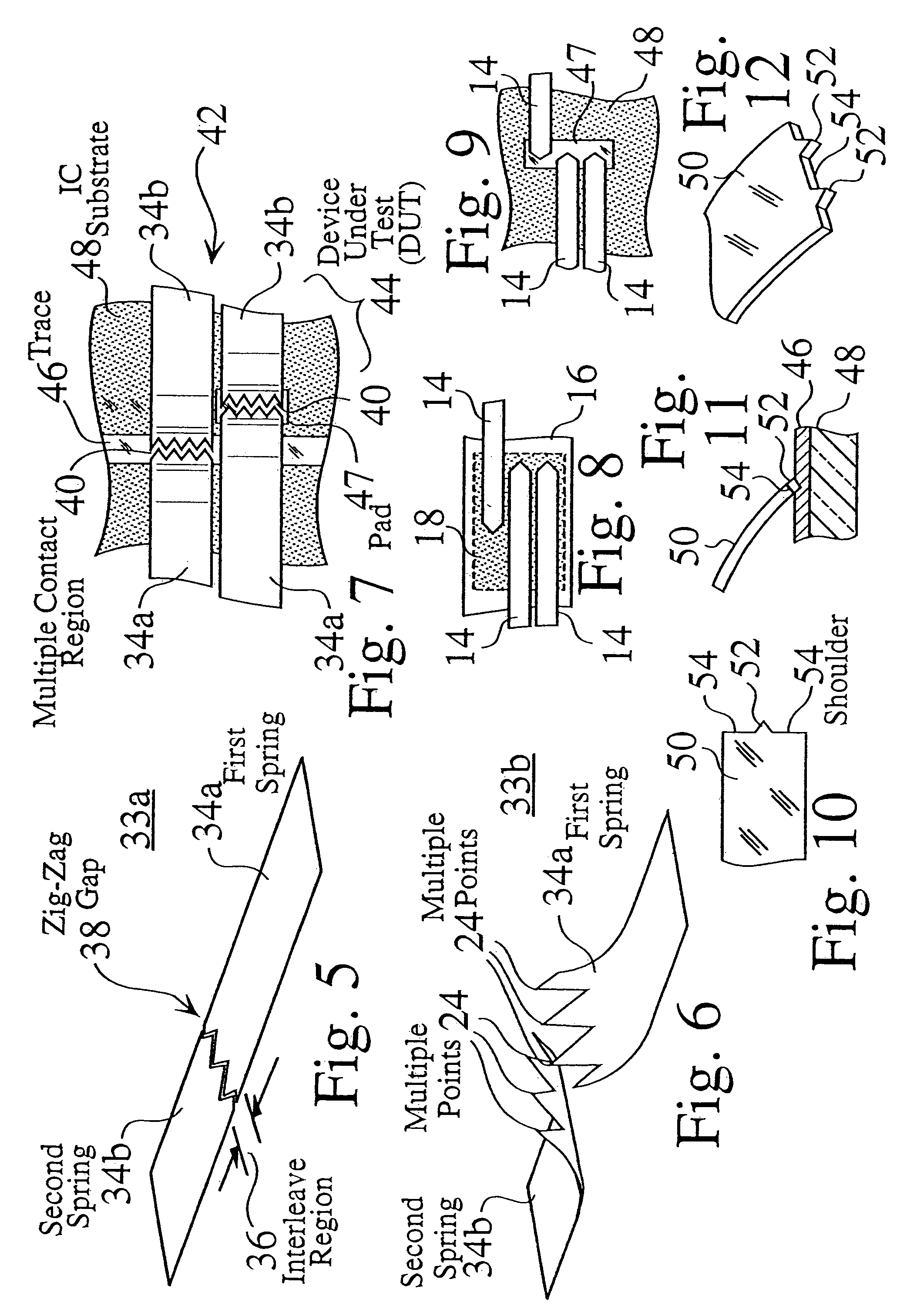
[0070]FIG. 1 is a plan view 10 of a linear array 12 of photolithographically patterned springs 14a–14n, prior to release from a substrate 16. The conductive springs 14a–14n are typically formed on the substrate layer 16, by successive layers of deposited metal 17 (e.g. such as layers 17a, 17b in FIG. 13), such as through low and high energy plasma and sputter deposition processes, followed by photolithographic patterning, as is widely known in the semiconductor industry. The successive layers 17 have different inherent levels of stress. The release regions 18 of the substrate 16 are then processed by undercut etching, whereby portions of the spring contacts 14a–14n, which are located over the release regions 18, are released from the substrate 16 and extend (i.e. bend) away from the substrate 16, as a result of the inherent stresses between the deposited metallic layers. Fixed regions 15 (FIG. 3, FIG. 4) of the deposited metal traces remain affixed to the substrate 16, and are typic...


PUM


Abstract

Several embodiments of massively parallel interface structures are disclosed, which may be used in a wide variety of permanent or temporary applications, such as for interconnecting integrated circuits (ICs) to test and burn-in equipment, for interconnecting modules within electronic devices, for interconnecting computers and other peripheral devices within a network, or for interconnecting other electronic circuitry. Preferred embodiments of the massively parallel interface structures provide massively parallel integrated circuit test assemblies. The massively parallel interface structures preferably use one or more substrates to establish connections between one or more integrated circuits on a semiconductor wafer, and one or more test modules. One or more layers on the intermediate substrates preferably include MEMS and / or thin-film fabricated spring probes. The parallel interface assemblies provide tight signal pad pitch and compliance, and preferably enable the parallel testing or burn-in of multiple ICs, using commercial wafer probing equipment. In some preferred embodiments, the parallel interface assembly structures include separable standard electrical connector components, which reduces assembly manufacturing cost and manufacturing time. These structures and assemblies enable high speed testing in wafer form.

Description

CROSS-REFERENCE TO RELATED APPLICATIONS[0001]This application is a divisional of U.S. Ser. No. 09 / 979,551, now U.S. Pat. No. 6,812,718 filed Nov. 21, 2001, and claims priority of International Patent Application No. PCT / US00 / 14768, filed May 26, 2000, and U.S. Provisional Application 60 / 136,637, filed May 27, 1999, all of which are incorporated herein in their entirety by this reference thereto.FIELD OF THE INVENTION[0002]The invention relates to the field of integrated circuit (IC) testing and burn-in structures and processes, as well as high bandwidth electronic systems. More particularly, the invention relates to improvements in photolithography-patterned spring contacts and enhanced system interconnect assemblies having photolithography-patterned spring contacts for use in the testing or burn-in of integrated circuits and interconnecting a large number of signals between electronic systems or subsystems.BACKGROUND OF THE INVENTION[0003]Integrated circuits are typically tested in...

Claims


Application Information

Patent Timeline
Patent Type & Authority Patents(United States)
IPC IPC(8): G01R31/02G01R31/26G01R31/28
CPCG01R1/07342G01R3/00G01R31/2889G01R31/2863G01R31/2874G01R1/06722
Inventor CHONG, FU CHIUNGMOK, SAMMY
Owner ADVANTEST SINGAPORE PTE LTD
Why Eureka
Try Eureka